K4B4G1646Q View Datasheet(PDF) - Samsung
Part Name
Description
Manufacturer
K4B4G1646Q Datasheet PDF : 65 Pages
| |||
K4B4G1646Q
datasheet
Preliminary Rev. 0.5
DDR3L SDRAM
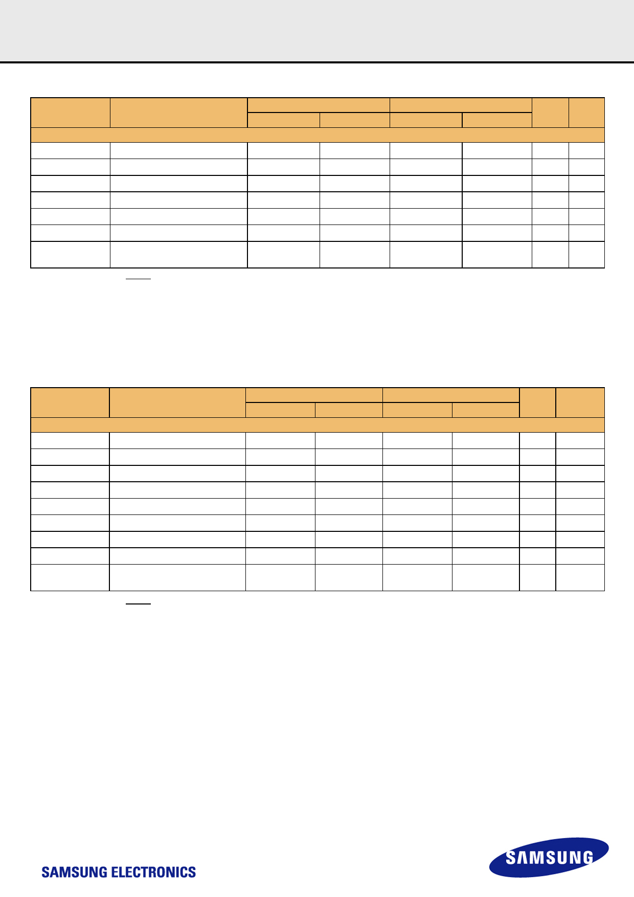
[ Table 9 ] Single-ended AC & DC input levels for DQ and DM (1.35V)
Symbol
Parameter
DDR3L-800/1066
Min.
Max.
DDR3L-1333/1600
Min.
Max.
Unit NOTE
1.35V
VIH.DQ(DC90) DC input logic high
VREF + 90
VDD
VREF + 90
VDD
mV
1
VIL.DQ(DC90)
VIH.DQ(AC160)
VIL.DQ(AC160)
VIH.DQ(AC135)
DC input logic low
AC input logic high
AC input logic low
AC input logic high
VSS
VREF + 160
Note 2
VREF + 135
VREF - 90
Note 2
VREF - 160
Note 2
VSS
-
-
VREF + 135
VREF - 90
-
-
Note 2
mV
1
mV 1,2,5
mV 1,2,5
mV 1,2,5
VIL.DQ(AC135) AC input logic low
Note 2
VREF - 135
Note 2
VREF - 135
mV 1,2,5
VREFDQ(DC)
Reference Voltage for DQ, DM
inputs
0.49*VDD
0.51*VDD
0.49*VDD
0.51*VDD
V
3,4
NOTE :
1. For input only pins except RESET, VREF = VREFDQ(DC)
2. See "Overshoot and Undershoot specifications" section.
3. The ac peak noise on VRef may not allow VRef to deviate from VRefDQ(DC) by more than +/-1% VDD (for reference: approx. +/- 13.5 mV).
4. For reference: approx. VDD/2 +/- 13.5 mV.
5. These levels apply for 1.35 Volt operation only. If the device is operated at 1.5 V, the respective levels in JESD79-3 ( VIH/L.DQ(DC100), VIH/L.DQ(AC175), VIH/
L.DQ(AC150), VIH/L.DQ(AC135), etc. ) apply. The 1.5 V levels (VIH/L.DQ(DC100), VIH/L.DQ(AC175), VIH/L.DQ(AC150), VIH/L.DQ(AC135), etc. ) do not apply when the
device is operated in the 1.35 voltage range.
[ Table 10 ] Single-ended AC & DC input levels for DQ and DM (1.5V)
Symbol
Parameter
DDR3-800/1066
Min.
Max.
DDR3-1333/1600
Min.
Max.
Unit
NOTE
1.5V
VIH.DQ(DC100)
VIL.DQ(DC100)
VIH.DQ(AC175)
VIL.DQ(AC175)
VIH.DQ(AC150)
DC input logic high
DC input logic low
AC input logic high
AC input logic low
AC input logic high
VREF + 100
VSS
VREF + 175
NOTE 2
VREF + 150
VDD
VREF - 100
NOTE 2
VREF - 175
NOTE 2
VREF + 100
VSS
-
-
VREF + 150
VDD
mV
VREF - 100
mV
-
mV
-
mV
NOTE 2
mV
1,5
1,6
1,2,7
1,2,8
1,2,7
VIL.DQ(AC150)
VIH.DQ(AC135)
VIL.DQ(AC135)
VREFDQ(DC)
AC input logic low
AC input logic high
AC input logic low
Reference Voltage for DQ, DM
inputs
NOTE 2
VREF + 135
NOTE 2
0.49*VDD
VREF - 150
NOTE 2
VREF - 135
0.51*VDD
NOTE 2
VREF + 135
NOTE 2
0.49*VDD
VREF - 150
NOTE 2
VREF - 135
0.51*VDD
mV
1,2,8
mV 1,2,7,10
mV 1,2,8,10
V
3,4,9
NOTE :
1. For input only pins except RESET, VREF = VREFDQ(DC)
2. See "Overshoot and Undershoot specifications" section.
3. The ac peak noise on VRef may not allow VRef to deviate from VRefDQ(DC) by more than +/-1% VDD (for reference: approx. +/- 15 mV).
4. For reference: approx. VDD/2 +/- 15 mV.
5. VIH(dc) is used as a simplified symbol for VIH.DQ(DC100)
6. VIL(dc) is used as a simplified symbol for VIL.DQ(DC100)
7. VIH(ac) is used as a simplified symbol for VIH.DQ(AC175), VIH.DQ(AC150), and VIH.DQ(AC135); VIH.DQ(AC175) value is used when Vref + 0.175V is referenced,
VIH.DQ(AC150) value is used when Vref + 0.150V is referenced, and VIH.DQ(AC135) value is used when Vref + 0.135V is referenced.
8. VIL(ac) is used as a simplified symbol for VIL.DQ(AC175), VIL.DQ(AC150), and VIL.DQ(AC135); VIL.DQ(AC175) value is used when Vref - 0.175V is referenced,
VIL.DQ(AC150) value is used when Vref - 0.150V is referenced, and VIL.DQ(AC135) value is used when Vref - 0.135V is referenced.
9. VrefCA(DC) is measured relative to VDD at the same point in time on the same device
10. Optional in DDR3 SDRAM for DDR3-800/1066/1333/1600: Users should refer to the DRAM supplier data sheetand/or the DIMM SPD to determine if DDR3 SDRAM devices
support this option.
- 12 -
Share Link: 