ADF7021_06 View Datasheet(PDF) - Analog Devices
Part Name
Description
Manufacturer
ADF7021_06 Datasheet PDF : 44 Pages
| |||
Preliminary Technical Data
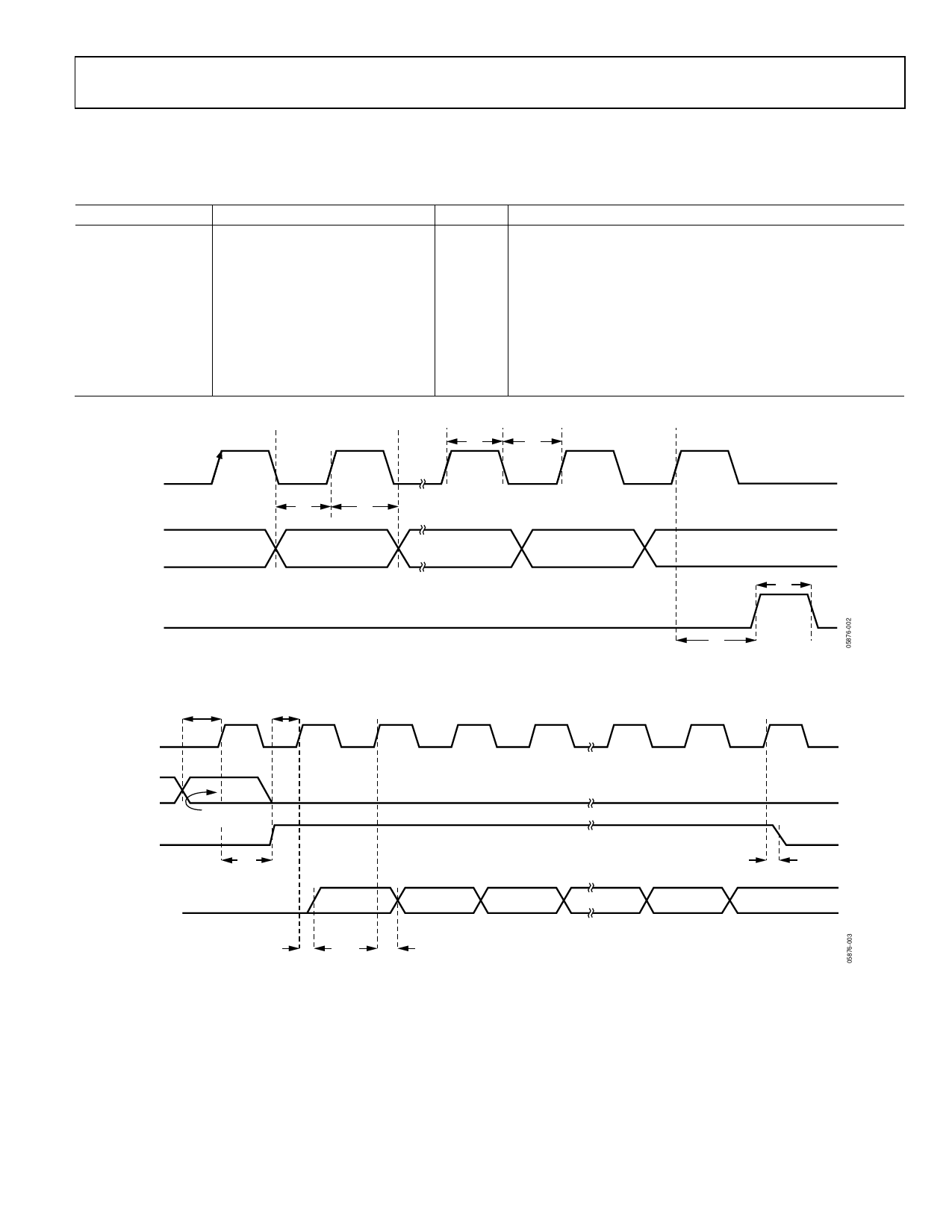
TIMING CHARACTERISTICS
VDD = 3 V ± 10%, VGND = 0 V, TA = 25°C, unless otherwise noted. Guaranteed by design, but not production tested.
Table 2.
Parameter
t1
t2
t3
t4
t5
t6
t8
t9
t10
Limit at TMIN to TMAX
<10
<10
<25
<25
<10
<20
<25
<25
<10
Unit
Test Conditions/Comments
ns
SDATA to SCLK setup time
ns
SDATA to SCLK hold time
ns
SCLK high duration
ns
SCLK low duration
ns
SCLK to SLE setup time
ns
SLE pulse width
ns
SCLK to SREAD data valid, readback
ns
SREAD hold time after SCLK, readback
ns
SCLK to SLE disable time, readback
ADF7021
SCLK
SDATA
DB31 (MSB)
t1
t2
DB30
t3
t4
DB2
DB1
(CONTROL BIT C2)
SLE
t1
t2
SCLK
Figure 2. Serial Interface Timing Diagram
DB0 (LSB)
(CONTROL BIT C1)
t6
t5
SDATA
SLE
REG7 DB0
(CONTROL BIT C1)
t3
SREAD
t8
X
RV16
RV15
t9
Figure 3. Readback Timing Diagram
t10
RV2
RV1
Rev. PrI | Page 7 of 44
Share Link: 