S25FL127S(2005) View Datasheet(PDF) - Cypress Semiconductor
Part Name
Description
Manufacturer
S25FL127S Datasheet PDF : 131 Pages
| |||
S25FL127S
3.5.3
Clock Pulse Count
The device verifies that all program, erase, and Write Registers (WRR) commands consist of a clock pulse count that is a multiple of
eight before executing them. A command not having a multiple of 8 clock pulse count is ignored and no error status is set for the
command.
4. Electrical Specifications
4.1 Absolute Maximum Ratings
Table 4.1 Absolute Maximum Ratings
Storage Temperature Plastic Packages
Ambient Temperature with Power Applied
VCC
Input voltage with respect to Ground (VSS) (Note 1)
Output Short Circuit Current (Note 2)
-65°C to +150°C
-65°C to +125°C
-0.5V to +4.0V
-0.5V to +(VCC + 0.5V)
100 mA
Notes:
1. See Input Signal Overshoot on page 26 for allowed maximums during signal transition.
2. No more than one output may be shorted to ground at a time. Duration of the short circuit should not be greater than one second.
3. Stresses above those listed under Absolute Maximum Ratings may cause permanent damage to the device. This is a stress rating only; functional operation of the
device at these or any other conditions above those indicated in the operational sections of this data sheet is not implied. Exposure of the device to absolute maximum
rating conditions for extended periods may affect device reliability.
4.2 Operating Ranges
Operating ranges define those limits between which the functionality of the device is guaranteed.
4.2.1
Temperature Ranges
Industrial (I) Devices
Ambient Temperature (TA)
Industrial Plus (V) Device
-40°C to +85°C
Ambient Temperature (TA) -40°C to +105°C
Industrial Plus operating and performance parameters will be determined by device characterization and may vary from standard
industrial temperature range devices as currently shown in this specification.
4.2.2
VCC
Power Supply Voltage
2.7V to 3.6V
4.2.3
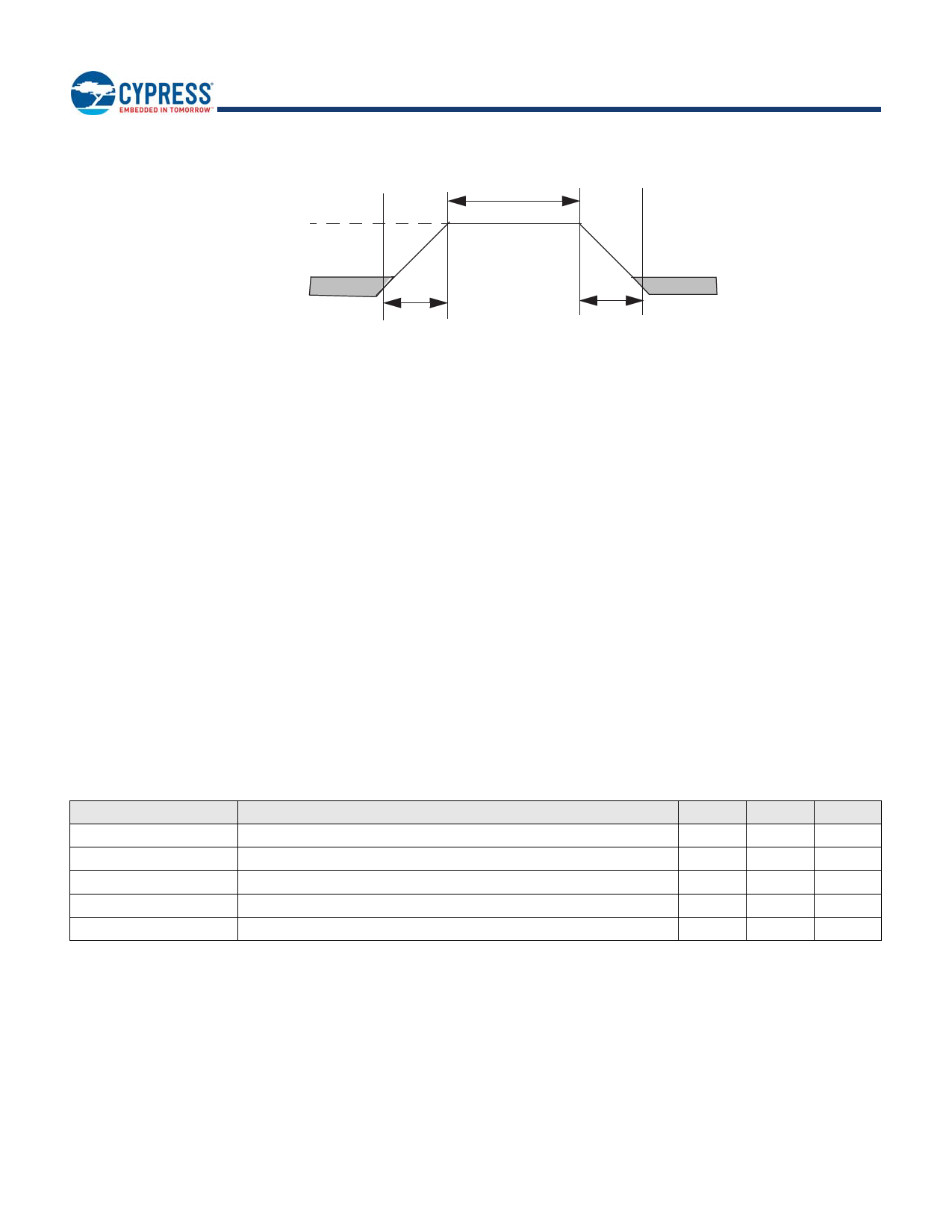
Input Signal Overshoot
During DC conditions, input or I/O signals should remain equal to or between VSS and VCC. During voltage transitions, inputs or I/Os
may overshoot VSS to –2.0V or overshoot to VCC +2.0V, for periods up to 20 ns.
Document Number: 001-98282 Rev. *F
Page 26 of 130
Share Link: 