S25FL127SABMHI003(2005) View Datasheet(PDF) - Cypress Semiconductor
Part Name
Description
Manufacturer
S25FL127SABMHI003 Datasheet PDF : 131 Pages
| |||
S25FL127S
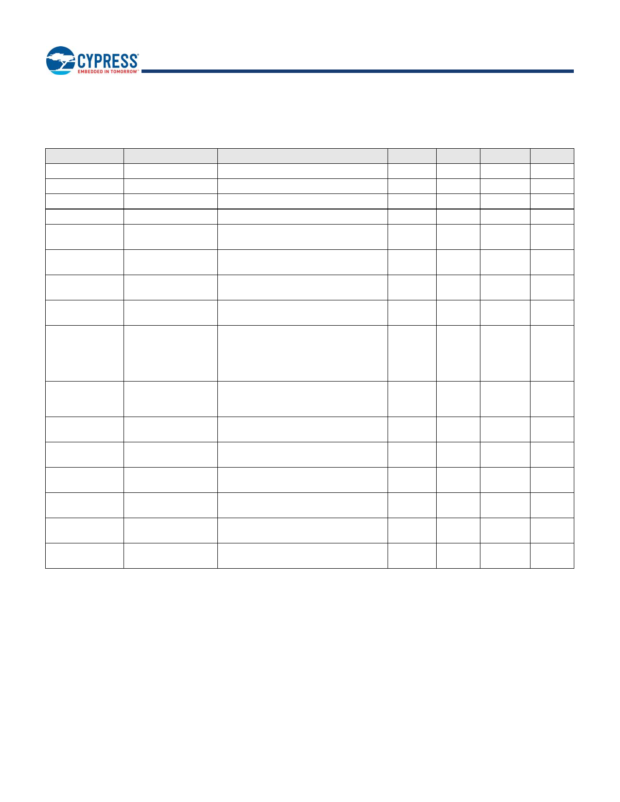
Table 4.2 Power-up/Power-down Voltage and Timing
Symbol
VCC (min)
VCC (cut-off)
VCC (low)
tPU
tPD
Parameter
VCC (minimum operation voltage)
VCC (Cut 0ff where re-initialization is needed)
VCC (low voltage for initialization to occur)
VCC (min) to Read operation
VCC (low) time
Min
Max
Unit
2.7
V
2.4
V
1.0
V
300
µs
1.0
µs
VCC
VCC(max)
VCC(min)
Figure 4.3 Power-up
tPU
Full Device Access
Time
VCC
VCC(max)
VCC(min)
VCC(cut-off)
Figure 4.4 Power-down and Voltage Drop
No Device Access Allowed
tPU Device Access
Allowed
VCC(low)
tPD
Time
Document Number: 001-98282 Rev. *F
Page 28 of 130
Share Link: 