IS43TR16640A(2016) View Datasheet(PDF) - Integrated Silicon Solution
Part Name
Description
Manufacturer
IS43TR16640A Datasheet PDF : 87 Pages
| |||
IS43/46TR16640A, IS43/46TR16640AL
IS43/46TR81280A, IS43/46TR81280AL
2.3.2.5 Write Recovery
The programmed WR value MR0 (bits A9, A10, and A11) is used for the auto precharge feature along with tRP to
determine tDAL. WR (write recovery for auto-precharge) min in clock cycles is calculated by dividing tWR (in ns) by tCK
(in ns) and rounding up to the next integer: WRmin[cycles] = Roundup(tWR[ns]/tCK[ns]). The WR must be programmed to
be equal to or larger than tWR(min).
2.3.2.6 Precharge PD DLL
MR0 (bit A12) is used to select the DLL usage during precharge power-down mode. When MR0 (A12 = 0), or ‘slow-exit’,
the DLL is frozen after entering precharge power-down (for potential power savings) and upon exit requires tXPDLL to be
met prior to the next valid command. When MR0 (A12 = 1), or ‘fast-exit’, the DLL is maintained after entering precharge
power-down and upon exiting power-down requires tXP to be met prior to the next valid command.
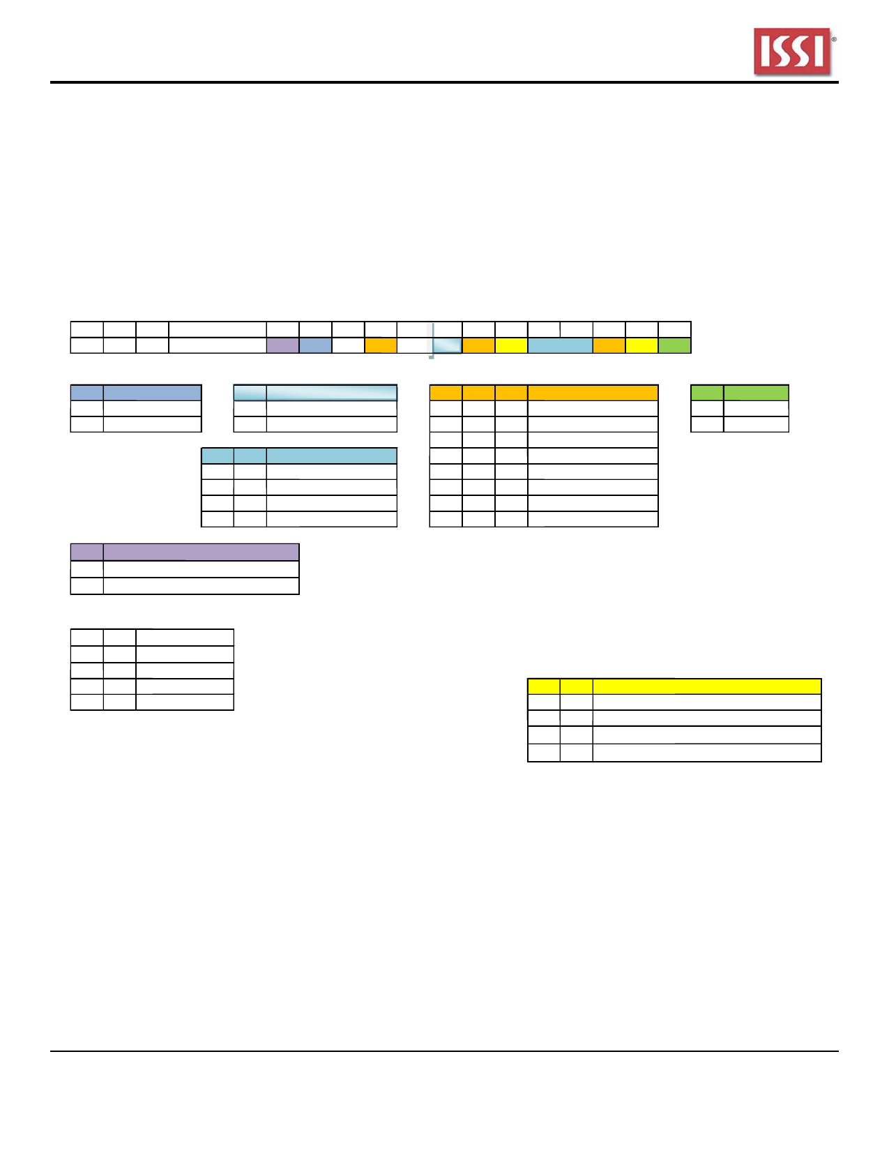
2.3.3 Mode Register MR1
The Mode Register MR1 stores the data for enabling or disabling the DLL, output driver strength, Rtt_Nom impedance,
additive latency, Write leveling enable, TDQS enable and Qoff. The Mode Register 1 is written by asserting low on CS#,
RAS#, CAS#, WE#, high on BA0 and low on BA1 and BA2, while controlling the states of address pins according to
Figure 2.3.3.
BA2 BA1 BA0
A13
A12 A11 A10 A9 A8 A7 A6 A5 A4 A3 A2 A1 A0 Address Field
00 1
0* 1
Qoff TDQS 0*1 Rtt 0*1 Level Rtt D.I.C AL
Rtt D.I.C DLL Mode Register 1
A11 TDQS enable
0
Disabled
1
Enabled
A7 Write leveling enable
0
Disabled
1
Enabled
A4 A3
00
01
10
11
Additive Latency
0 (AL disabled)
CL-1
CL-2
Reserved
A12
Qoff *2
0
Output buffer enabled
1
Output buffer disabled *2
*2: Outputs disabled - DQs, DQSs, DQS#s.
BA1 BA0
00
01
10
11
MR Select
MR0
MR1
MR2
MR3
A9 A6 A2
Rtt_Nom *3
A0
000
ODT disabled
0
001
RZQ/4
1
010
RZQ/2
011
100
RZQ/6
RZQ/12 *4
101
RZQ/8 *4
110
Reserved
111
Reserved
Note: RZQ = 240
*3:In Write leveling Mode (MR1[bit7] = 1) with
MR1[bit12]=1, all RTT_Nom settings are allowed; in
Write Leveling Mode (MR1[bit7] = 1) with
MR1[bit12]=0, only RTT_Nom settings of RZQ/2,
RZQ/4 and RZQ/6 are allowed.
*4:If RTT_Nom is used during Writes, only the
values RZQ/2, RZQ/4 and RZQ/6 are allowed.
DLL Enable
Enable
Disable
A5 A1
00
01
10
11
Output Driver Impedance Control
RZQ/6
RZQ/7
RZQ/TBD
RZQ/TBD
* 1 : A8, A10, and A13 must be programmed to 0 during MRS.
* TDQS must be disabled for x16 option.
Figure 2.3.3 MR1 Definition
Integrated Silicon Solution, Inc. – www.issi.com –
12
Rev. J
03/14/2016
Share Link: 