IS43TR16640A(2016) View Datasheet(PDF) - Integrated Silicon Solution
Part Name
Description
Manufacturer
IS43TR16640A Datasheet PDF : 87 Pages
| |||
IS43/46TR16640A, IS43/46TR16640AL
IS43/46TR81280A, IS43/46TR81280AL
support any half-clock latencies. The overall Write Latency (WL) is defined as Additive Latency (AL) + CAS Write Latency
(CWL); WL = AL + CWL. For more information on the supported CWL and AL settings based on the operating clock
frequency, refer to “Standard Speed Bins”.
2.3.4.3 Auto Self-Refresh (ASR) and Self-Refresh Temperature (SRT)
For more details refer to “Extended Temperature Usage”. DDR3 SDRAMs support Self-Refresh operation at all supported
temperatures. Applications requiring Self-Refresh operation in the Extended Temperature Range must use the ASR
function or program the SRT bit appropriately.
2.3.4.4 Dynamic ODT (Rtt_WR)
DDR3 SDRAM introduces a new feature “Dynamic ODT”. In certain application cases and to further enhance signal
integrity on the data bus, it is desirable that the termination strength of the DDR3 SDRAM can be changed without issuing
an MRS command. MR2 Register locations A9 and A10 configure the Dynamic ODT setings. In Write leveling mode, only
RTT_Nom is available. For details on Dynamic ODT operation, refer to “Dynamic ODT”.
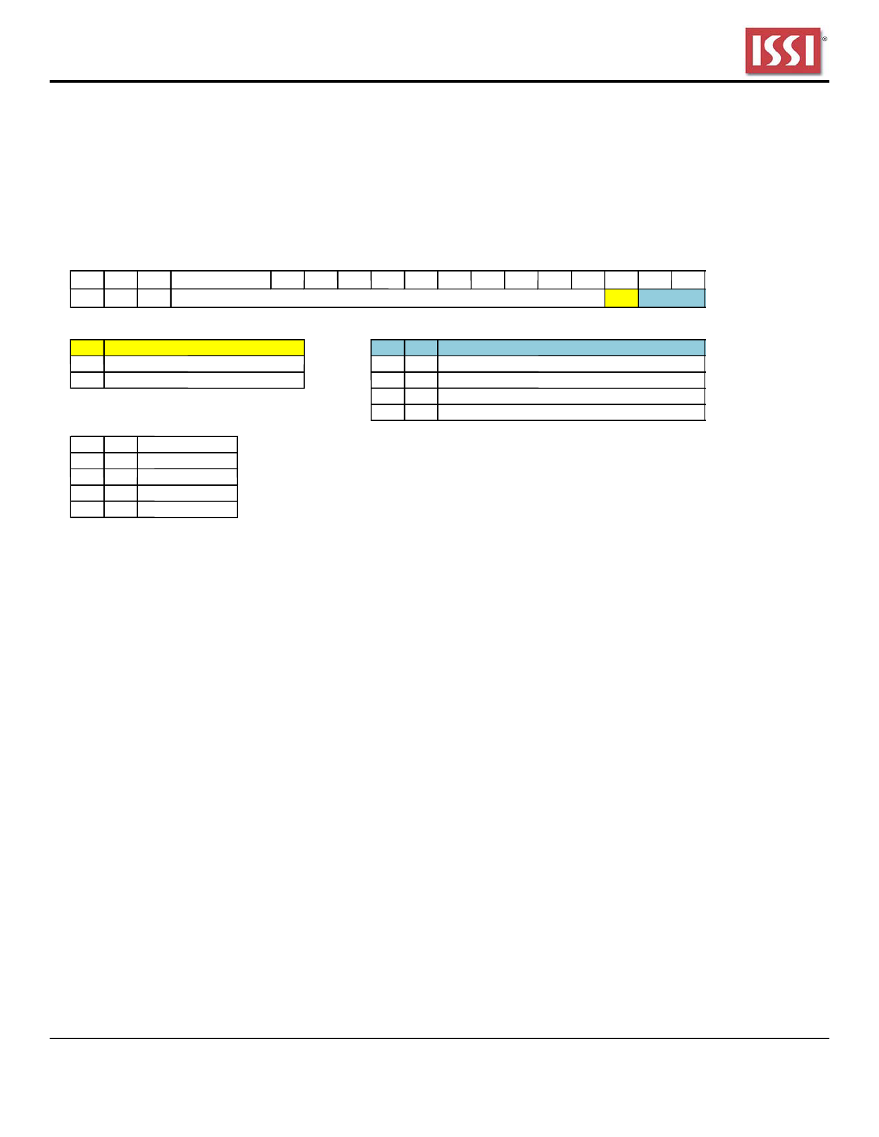
2.3.5 Mode Register MR3
The Mode Register MR3 controls Multi-purpose registers. The Mode Register 3 is written by asserting low on CS#, RAS#,
CAS#, WE#, high on BA1 and BA0, and low on BA2 while controlling the states of address pins according to the below.
BA2 BA1 BA0
A13
A12 A11 A10 A9 A8 A7 A6 A5 A4 A3 A2 A1 A0 Address Field
011
0* 1
MPR MPR Loc Mode Register 3
MRP Operation
A2
MPR
0
Normal operation *3
1
Dataflow from MPR
MPR Address
A1 A0
00
01
10
11
MPR location
Predefined pattern *2
RFU
RFU
RFU
BA1 BA0
00
01
10
11
MR Select
MR0
MR1
MR2
MR3
* 1 : A3 - A13 must be programmed to 0 during MRS.
* 2 : The predefined pattern will be used for read synchronization.
* 3 : When MPR control is set for normal operation (MR3 A[2] = 0) then MR3 A[1:0] will be ignored.
Figure 2.3.5 MR3 Definition
2.3.5.1 Multi-Purpose Register (MPR)
The Multi Purpose Register (MPR) function is used to Read out a predefined system timing calibration bit sequence. To
enable the MPR, a Mode Register Set (MRS) command must be issued to MR3 register with bit A2=1. Prior to issuing the
MRS command, all banks must be in the idle state (all banks precharged and tRP met). Once the MPR is enabled, any
subsequent RD or RDA commands will be redirected to the Multi Purpose Register. When the MPR is enabled, only RD
or RDA commands are allowed until a subsequent MRS command is issued with the MPR disabled (MR3 bit A2=0).
Power down mode, Self-Refresh and any other non-RD/RDA command is not allowed during MPR enable mode. The
RESET function is supported during MPR enable mode.
The Multi Purpose Register (MPR) function is used to Read out a predefined system timing calibration bit sequence. The
basic concept of the MPR is shown in Figure 2.3.5.1.
Integrated Silicon Solution, Inc. – www.issi.com –
15
Rev. J
03/14/2016
Share Link: 