LC75893M View Datasheet(PDF) - SANYO -> Panasonic
Part Name
Description
Manufacturer
LC75893M Datasheet PDF : 23 Pages
| |||
LC75893M
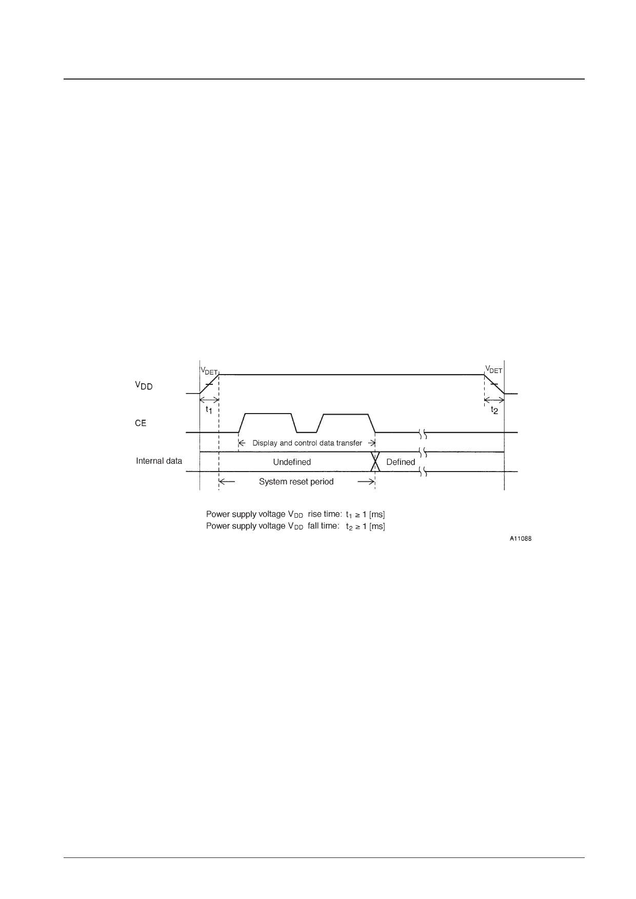
Voltage Detection Type Reset Circuit (VDET)
This circuit generates an output signal and resets the system when power is first applied and when the voltage drops, i.e.,
when the power supply voltage is less than or equal to the power down detection voltage VDET, which is 3.0 V, typical.
To assure that this function operates reliably, a capacitor must be added to the power supply line so that the power supply
voltage VDD rise time when power is first applied and the power supply voltage VDD fall time when the voltage drops are
both at least 1 ms. (See Figure 3.)
System Reset
The LC75893M supports the reset method described below. When a system reset is applied, display is turned off, key
scanning is stopped, and all the key data is reset to low. When the reset is cleared, display is turned on and key scanning
become possible.
1. Reset method
If at least 1 ms is assured as the supply voltage VDD rise time when power is applied, a system reset will be applied by
the VDET output signal when the supply voltage is brought up. If at least 1 ms is assured as the supply voltage VDD
fall time when power drops, a system reset will be applied in the same manner by the VDET output signal when the
supply voltage is lowered. Note that the reset is cleared at the point when all the serial data (the display data D1 to
D48 and the control data) has been transferred, i.e., on the fall of the CE signal on the transfer of the last direction
data, after all the direction data has been transferred. (See Figure 3.)
Figure 3
2. LC75893M internal block states during the reset period
• CLOCK GENERATOR
Reset is applied and the base clock is stopped. However the OSC pin state (normal or sleep mode) is determined
after the S0 and S1 control data bits are transferred.
• COMMON DRIVER, SEGMENT DRIVER & LATCH
Reset is applied and the display is turned off. However, display data can be input to the latch circuit in this state.
• KEY SCAN
Reset is applied, the circuit is set to the initial state, and at the same time the key scan operation is disabled.
• KEY BUFFER
Reset is applied and all the key data is set to low.
• CCB INTERFACE, CONTROL REGISTER, SHIFT REGISTER
Since serial data transfer is possible, these circuits are not reset.
No. 5971-15/23
Share Link: 