CXD2460R View Datasheet(PDF) - Sony Semiconductor
Part Name
Description
Manufacturer
CXD2460R Datasheet PDF : 36 Pages
| |||
CXD2460R
Detailed description
Operation control settings
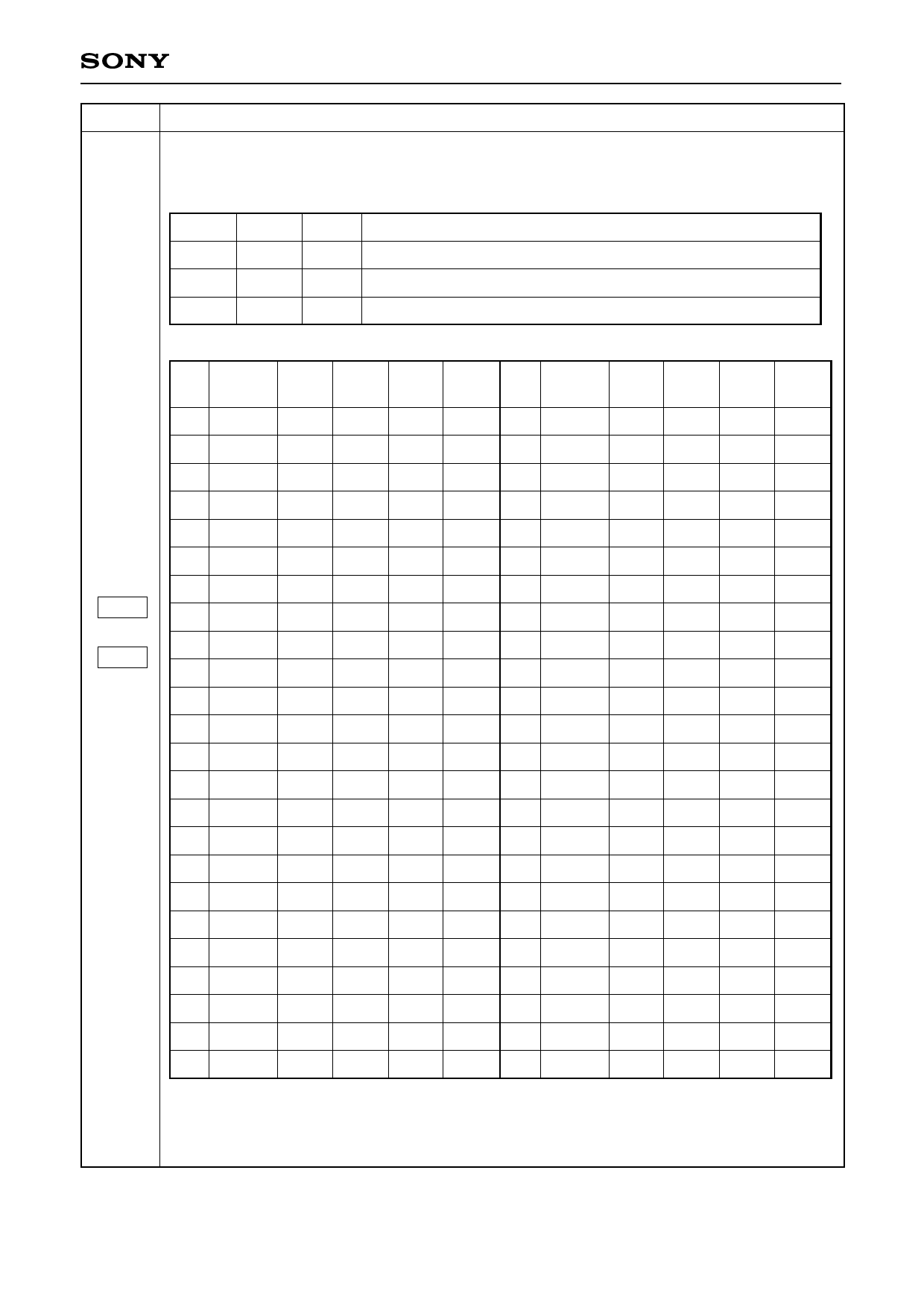
The operating mode control bits are loaded to the CXD2460R at the rise timing of the SEN input,
and control is applied immediately.
D19 D18 Symbol
Control mode
0
0 CAM Normal operation mode
0
1 SLP Sleep mode (mode for the status where CCD drive is not required)
1
X STN Standby mode
Pin status during operation control
Pin
No.
Symbol
CAM
SLP
STN
RST∗
Pin
No.
Symbol
CAM
SLP
STN RST∗
1 CKO ACT ACT ACT ACT 25 MCK ACT ACT ACT ACT
2 VSS0
—
—
—
— 26 VDD1
————
3 CKI
ACT ACT ACT ACT 27 2MCK ACT ACT ACT ACT
4 OSCO ACT ACT ACT ACT 28 TEST2 —
—
—
—
5 OSCI ACT ACT ACT ACT 29 SEN
ACT ACT —
—
6 VDD0
—
—
—
— 30 SSK
ACT ACT —
—
7 TEST1 —
—
—
— 31 SSI
ACT ACT —
—
D17
8 AVD0
—
—
—
— 32 ID
ACT L
L
L
to
9 RG
ACT L
L
L 33 EXP
ACT L
L
L
D18
STB
10 VSS1
—
—
—
— 34 HRO ACT ACT L
L
11 VSS2
—
—
—
— 35 FRO
ACT ACT L
L
12 H1
ACT L
L
L
36 VSS4
————
13 H2
ACT L
L
L 37 HRI
ACT ACT —
—
14 AVD1 — — — — 38 FRI
ACT ACT —
—
15 XCPDM ACT L
L
L 39 VM
————
16 AVD2 — — — — 40 V1
ACT VM VM VM
17 XSHP ACT L
L
L 41 V3
ACT VM VM VM
18 XSHD ACT L
L
L 42 V2A
ACT VH VH VH
19 XRS ACT L
L
L 43 VH
————
20 VSS3
—
—
—
— 44 V2B
ACT VH VH VH
21 PBLK ACT L
L
L 45 SUB ACT VH VH VH
22 XCPOB ACT L
L
L 46 VL
————
23 ADCLK ACT L
L
L 47 DSGAT ACT ACT L
L
24 RST
ACT ACT ACT ACT 48 PS
ACT ACT ACT ACT
∗ See "6. RST pulse" for a detailed description of RST.
Note) ACT indicates circuit operation, and L indicates "low" output level in the controlled status.
For sleep mode or standby mode, stop supplying VH and VL power supplies with CCD
image sensor.
– 15 –
Share Link: 