CXD2460R View Datasheet(PDF) - Sony Semiconductor
Part Name
Description
Manufacturer
CXD2460R Datasheet PDF : 36 Pages
| |||
CXD2460R
Detailed description
D30 0: Normal operation
XVCK 1: V1, V2 and V3 are inverted and output as XV1, XV2 and XV3. The amplitude is from VL to VM.
D31
to
Invalid data
D39
CHKSUM
These are the checksum bits.
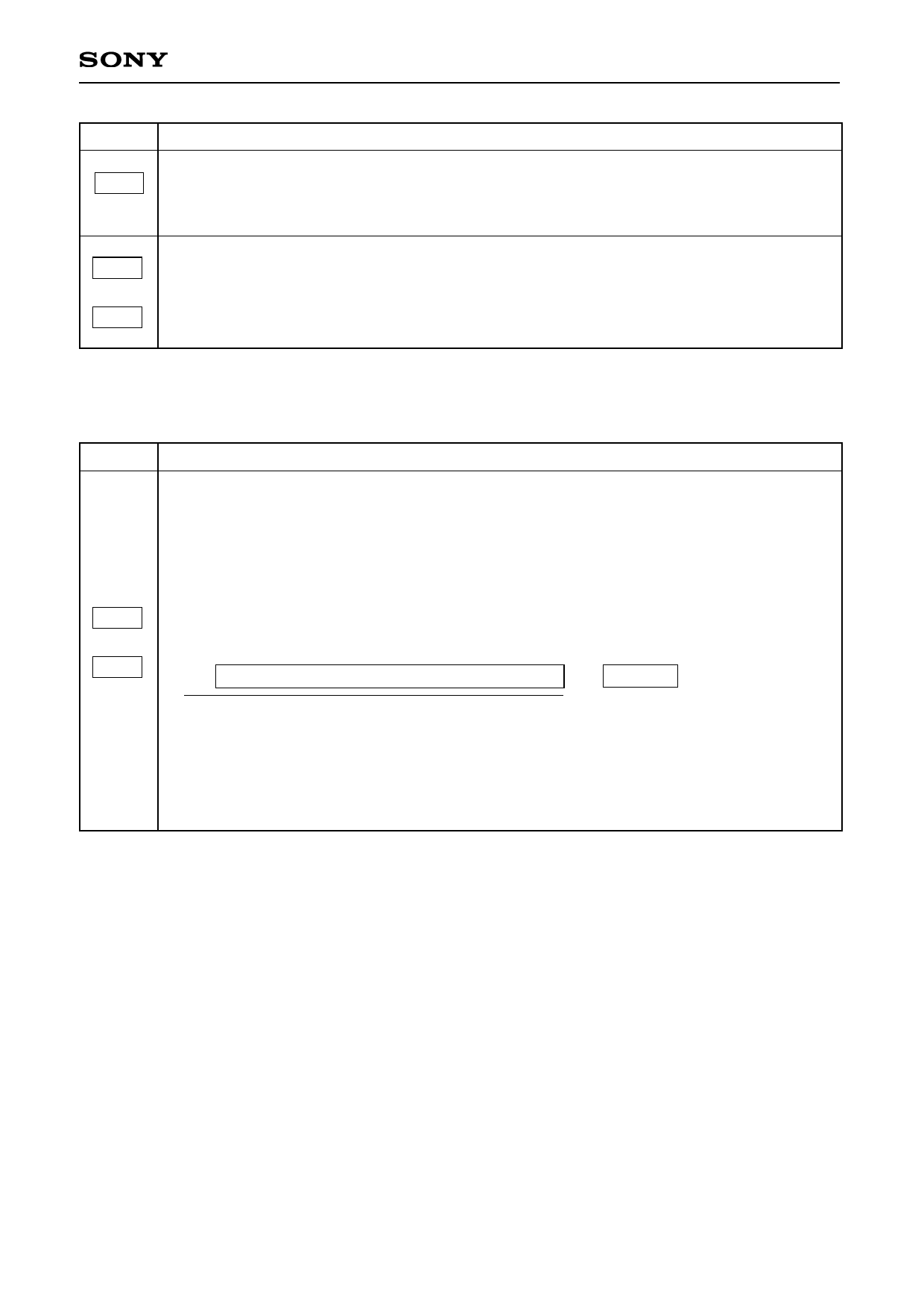
Detailed description
MSB
LSB
D07 D06 D05 D04 D03 D02 D01 D00
D15 D14 D13 D12 D11 D10 D09 D08
D23 D22 D21 D20 D19 D18 D17 D16
D40
D31 D30 D29 D28 D27 D26 D25 D24
to
D39 D38 D37 D36 D35 D34 D33 D32
D47
+) D47 D46 D45 D44 D43 D42 D41 D40 → CHKSUM
If the total = 0, the checksum results are OK.
Serial data is loaded to the internal registers only when checksum is OK.
Data is not reflected to the registers if checksum is NG.
Also, when CHKSUM = 0, the checksum results are always OK and the data is reflected to the
registers.
– 19 –
Share Link: 