DSP56852PB View Datasheet(PDF) - Motorola => Freescale
Part Name
Description
Manufacturer
DSP56852PB Datasheet PDF : 44 Pages
| |||
Freescale Semiconductor, Inc.
Table 8. External Clock Operation Timing Requirements4
Operating Conditions: VSS = VSSIO = VSSA = 0V, VDD = 1.62-1.98V, VDDIO = VDDA = 3.0–3.6V, TA = –40° to +120°C, CL ≤ 50pF, fop = 120MHz
Characteristic
Symbol
Min
Typ
Max
Unit
Frequency of operation (external clock driver)1
fosc
0
—
240
MHz
Clock Pulse Width4
tPW
6.25
—
—
ns
External clock input rise time2, 4
trise
—
—
TBD
ns
External clock input fall time3, 4
tfall
—
—
TBD
ns
1. See Figure 9 for details on using the recommended connection of an external clock driver.
2. External clock input rise time is measured from 10 to 90 percent.
3. External clock input fall time is measured from 90 to 10percent.
4. Parameters listed are guaranteed by design.
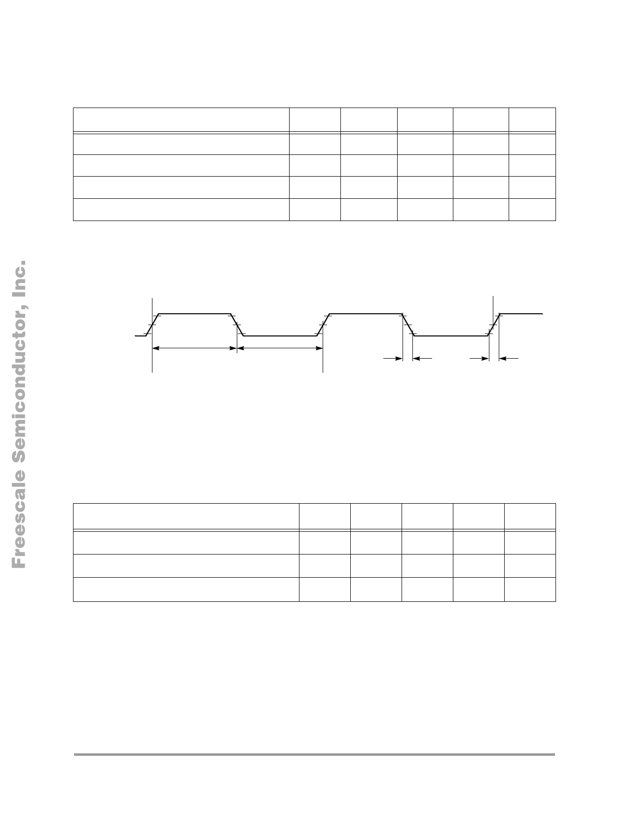
External
90%
Clock
50%
10% tPW
tPW
VIH
90%
50%
10%
tfall
trise
VIL
Note: The midpoint is VIL + (VIH – VIL)/2.
Figure 11. External Clock Timing
Table 9. PLL Timing
Operating Conditions: VSS = VSSIO = VSSA = 0V, VDD = 1.62-1.98V, VDDIO = VDDA = 3.0–3.6V, TA = –40° to +120°C, CL ≤ 50pF, fop = 120MHz
Characteristic
Symbol Min
Typ
Max
Unit
External reference crystal frequency for the PLL1
fosc
2
PLL output frequency
fclk
40
PLL stabilization time 2
tplls
—
4
4
MHz
—
240
MHz
1
10
ms
1. An externally supplied reference clock should be as free as possible from any phase jitter for the PLL to work correctly.
The PLL is optimized for 4MHz input crystal.
2. This is the minimum time required after the PLL setup is changed to ensure reliable operation.
20
DSP56852 Technical Data
For More Information On This Product,
Preliminary
Go to: www.freescale.com
Share Link: 