BU1425AK View Datasheet(PDF) - ROHM Semiconductor
Part Name
Description
Manufacturer
BU1425AK Datasheet PDF : 32 Pages
| |||
Multimedia ICs
BU1425AK / BU1425AKV
Table 5: Bit assignments in RGB Through mode
Output Pin
YOUT (45)
VOUT (39)
COUT (37)
BIT8
RD7
GD7
BD7
BIT7
RD6
GD6
BD6
BIT6
RD5
GD5
BD5
BIT5
RD4
GD4
BD4
BIT4
RD3
GD3
BD3
BIT3
RD2
GD2
BD2
BIT2
RD1
GD1
BD1
BIT1
RD0
GD0
BD0
BIT0
ROSD
GOSD
BOSD
The BU1425AK / AKV has an internal OSD switch and
chrominance data generating function. Consequently,
joint usage of an OSD-IC with blanking and R, G, and B
output can be easily supported by the OSD. Moreover,
a clock with half the internal processing frequency of
the BU1425AK is output from the PIXCLK pin, and can
be connected to the OSD-IC clock input, enabling the
timing to be captured.
ROSD, GOSD, and BOSD pin input is effective as long
as the OSDSW pin input is HIGH. The relationship
between OSD data and chrominance data is as shown
in Table 6 below.
Table 6: Correspondence between OSD function, input data and chrominance output
OSDSW
1
1
1
1
1
1
1
1
0
ROSD
0
0
0
0
1
1
1
1
∗
GOSD
0
0
1
1
0
0
1
1
∗
BOSD
0
1
0
1
0
1
0
1
∗
Output Chrominance Signal
Black (blanking)
Blue
Green
Cyan
Red
Magenta
Yellow
White
Based on input specified by IM0 and IM1
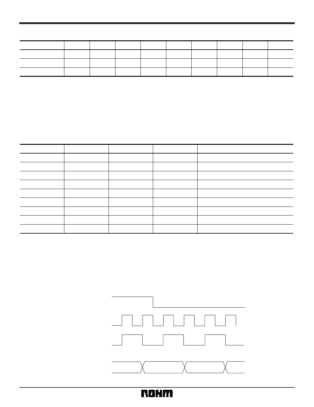
4) Clock modes
With the BU1425AK / AKV, clock input is available at the
VCLK pin.
Clocks supplied from an external source should basically
be input at a frequency double that of clocks used inter-
nally (basic clock: BCLK) (when the CLKSW pin is LOW).
The phase relationship between the internal clock and
HSY
the external clock at this time is as shown in Fig. 3, with
the HSY pin input serving as a reference. In the Master
mode, in which data from the HSY pin is output and
used, HSY is output at the timing shown in Fig. 3. With
the BU1425AK, data (RD, GD, BD, etc.) is read at the ris-
ing edge of the internal clock (BCLK), so data should be
input to the BU1425AK / AKV as shown in Fig. 3.
VCLK
Internal clock (BCLK)
Input data
Fig. 3 Illustration of clock timing (CLKSW is LOW)
13
Share Link: 