NT5SV16M8CT View Datasheet(PDF) - Nanya Technology
Part Name
Description
Manufacturer
NT5SV16M8CT Datasheet PDF : 66 Pages
| |||
NT5SV32M4CT
NT5SV16M8CT
NT5SV8M16CT
128Mb Synchronous DRAM
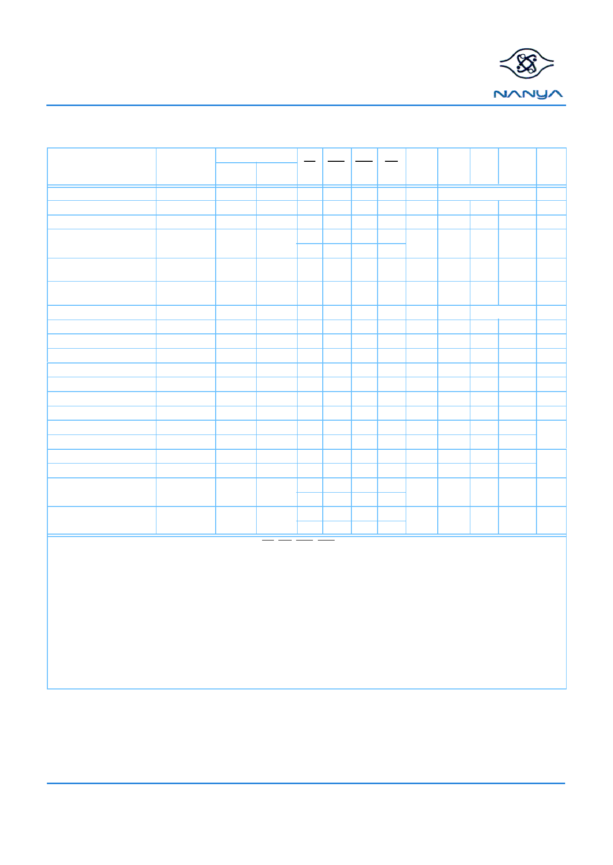
Command Truth Table (See note 1)
Function
CKE
Device State Previous Current CS
Cycle
Cycle
RAS CAS WE
DQM
BS0,
BS1
A10
A11,
A11,
A9-A0
Notes
Mode Register Set
Idle
H
X
L
L
L
L
X
OP Code
Auto (CBR) Refresh
Idle
H
H
L
L
L
H
X
X
X
X
Entry Self Refresh
Idle
H
L
L
L
L
H
X
X
X
X
Exit Self Refresh
Idle (Self-
Refresh)
H
X
X
X
L
H
X
X
X
X
L
H
H
H
Single Bank Precharge
See Current
State Table
H
X
L
L
H
L
X
BS
L
X
2
Precharge all Banks
See Current
State Table
H
X
L
L
H
L
X
X
H
X
Bank Activate
Idle
H
X
L
L
H
H
X
BS Row Address
2
Write
Active
H
X
L
H
L
L
X
BS
L Column 2
Write with Auto-Precharge Active
H
X
L
H
L
L
X
BS
H Column 2
Read
Active
H
X
L
H
L
H
X
BS
L Column 2
Read with Auto-Precharge Active
H
X
L
H
L
H
X
BS
H Column 2
Reserved
H
X
L
H
H
L
X
X
X
X
No Operation
Any
H
X
L
H
H
H
X
X
X
X
Device Deselect
Any
H
X
H
X
X
X
X
X
X
X
Clock Suspend Mode Entry Active
Clock Suspend Mode Exit Active
H
L
X
X
X
X
X
X
X
X
4
L
H
X
X
X
X
X
X
X
X
Data Write/Output Enable
Data Mask/Output Disable
Active
Active
H
X
X
X
X
X
L
X
X
X
5
H
X
X
X
X
X
H
X
X
X
Power Down Mode Entry Idle/Active
H
X
X
X
H
L
X
X
X
X
6, 7
L
H
H
H
Power Down Mode Exit
Any (Power
Down)
L
H
X
X
X
H
X
X
X
X
6, 7
L
H
H
H
1. All of the SDRAM operations are defined by states of CS, WE, RAS , CAS , and DQM at the positive rising edge of the clock.Refer to the
Current State Truth Table.
2. Bank Select (BS0, BS1): BS0, BS1 = 0,0 selects bank 0; BS0, BS1 = 1,0 selects bank 1; BS0, BS1 = 0,1 selects bank 2; BS0, BS1 = 1,1
selects bank 3.
3. Not applicable.
4. During normal access mode, CKE is held high and CK is enabled. When it is low, it freezes the internal clock and extends data Read and
Write operations. One clock delay is required for mode entry and exit.
5. The DQM has two functions for the data DQ Read and Write operations. During a Read cycle, when DQM goes high at a clock timing the
data outputs are disabled and become high impedance after a two-clock delay. DQM also provides a data mask function for Write cycles.
When it activates, the Write operation at the clock is prohibited (zero clock latency).
6. All banks must be precharged before entering the Power Down Mode. (If this command is issued during a burst operation, the device
state will be Clock Suspend Mode.) The Power Down Mode does not perform any refresh operations; therefore the device can’t remain in
this mode longer than the Refresh period (tREF) of the device. One clock delay is required for mode entry and exit.
7. A No Operation or Device Deselect Command is required on the next clock edge following CKE going high.
REV 1.0
May, 2001
29
© NANYA TECHNOLOGY CORP. All rights reserved.
NANYA TECHNOLOGY CORP. reserves the right to change Products and Specifications without notice.
Share Link: 