NT5SV16M8CT View Datasheet(PDF) - Nanya Technology
Part Name
Description
Manufacturer
NT5SV16M8CT Datasheet PDF : 66 Pages
| |||
NT5SV32M4CT
NT5SV16M8CT
NT5SV8M16CT
128Mb Synchronous DRAM
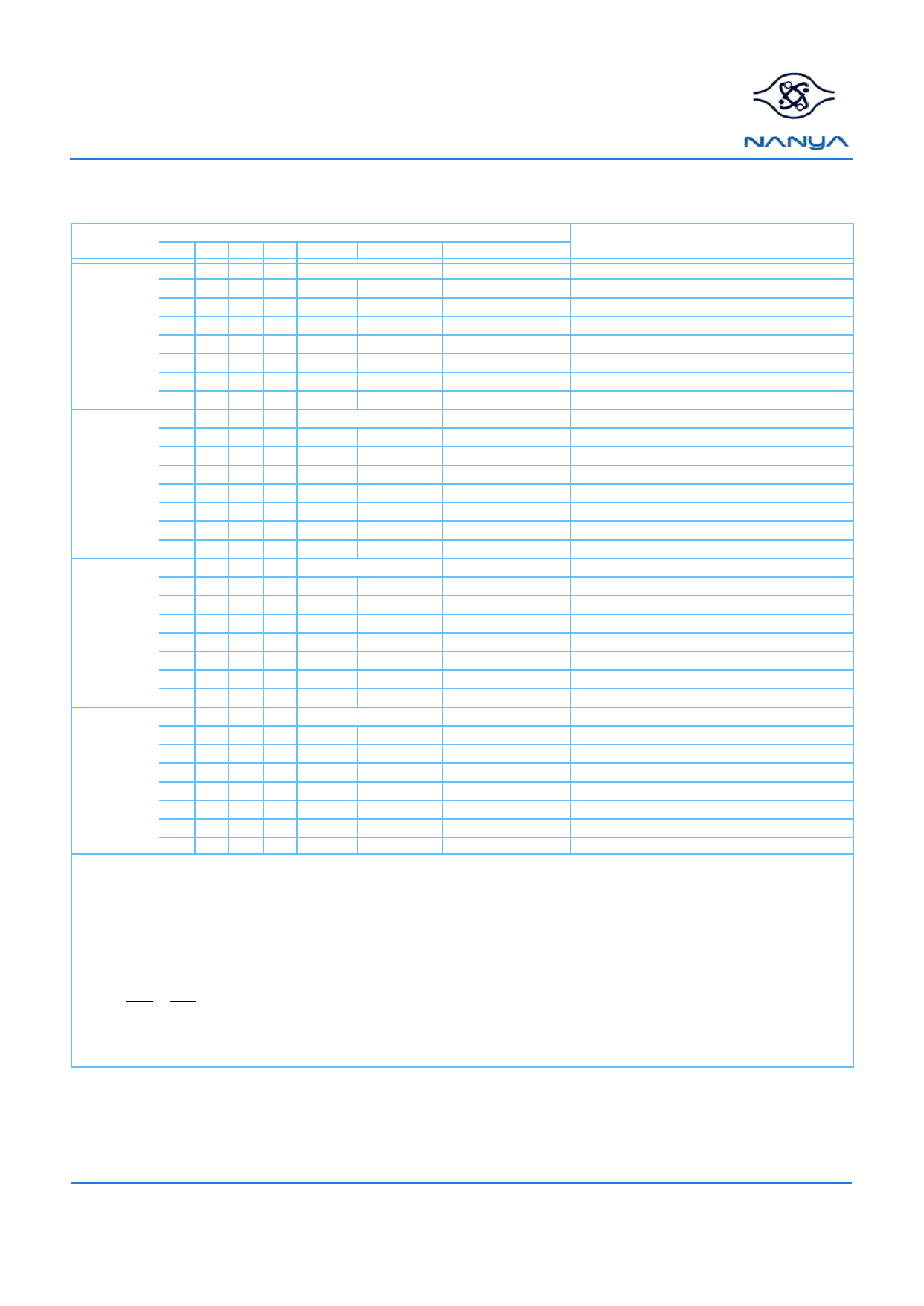
Current State Truth Table (Part 1 of 3)(See note 1)
Command
Current State
CS RAS CAS WE BS0,BS1 A11 - A0
Description
Action
LLL L
OP Code
Mode Register Set Set the Mode Register
LLLH
X
X
Auto or Self Refresh Start Auto or Self Refresh
LLH L
BS
X
Precharge
No Operation
L LHH
BS Row Address Bank Activate
Activate the specified bank and row
Idle
LHL L
BS
Column Write w/o Precharge ILLEGAL
LHL H
BS
Column Read w/o Precharge ILLEGAL
LHHH
X
X
No Operation
No Operation
HX XX
X
X
Device Deselect
No Operation or Power Down
LLL L
OP Code
Mode Register Set ILLEGAL
LLLH
X
X
Auto or Self Refresh ILLEGAL
LLH L
BS
X
Precharge
Precharge
L LHH
Row Active
LHL L
BS Row Address Bank Activate
BS
Column Write
ILLEGAL
Start Write; Determine if Auto Precharge
LHL H
BS
Column Read
Start Read; Determine if Auto Precharge
LHHH
X
X
No Operation
No Operation
HX XX
X
X
Device Deselect
No Operation
LLL L
OP Code
Mode Register Set ILLEGAL
LLLH
X
X
Auto or Self Refresh ILLEGAL
LLH L
BS
X
Precharge
Terminate Burst; Start the Precharge
Read
L LHH
LHL L
BS Row Address Bank Activate
BS
Column Write
ILLEGAL
Terminate Burst; Start the Write cycle
LHL H
BS
Column Read
Terminate Burst; Start a new Read cycle
LHHH
X
X
No Operation
Continue the Burst
HX XX
X
X
Device Deselect
Continue the Burst
LLL L
OP Code
Mode Register Set ILLEGAL
LLLH
X
X
Auto or Self Refresh ILLEGAL
LLH L
BS
X
Precharge
Terminate Burst; Start the Precharge
Write
L LHH
LHL L
BS Row Address Bank Activate
BS
Column Write
ILLEGAL
Terminate Burst; Start a new Write cycle
LHL H
BS
Column Read
Terminate Burst; Start the Read cycle
LHHH
X
X
No Operation
Continue the Burst
HX XX
X
X
Device Deselect
Continue the Burst
Notes
2
2, 3
4
4
5
6
4
7, 8
7, 8
4
8, 9
8, 9
4
8, 9
8, 9
1. CKE is assumed to be active (high) in the previous cycle for all entries. The Current State is the state of the bank that the Command is
being applied to.
2. All Banks must be idle; otherwise, it is an illegal action.
3. If CKE is active (high) the SDRAM will start the Auto (CBR) Refresh operation, if CKE is inactive (low) than the Self Refresh mo de is
entered.
4. The Current State refers to only one of the banks. If BS selects this bank then the action is illegal. If BS selects the bank not being refer-
enced by the Current State then the action may be legal depending on the state of that bank.
5. If CKE is inactive (low) then the Power Down mode is entered; otherwise there is a No Operation.
6. The minimum and maximum Active time (t RAS) must be satisfied.
7. The RAS to CAS Delay (tRCD ) must occur before the command is given.
8. Column address A10 is used to determine if the Auto Precharge function is activated.
9. The command must satisfy any bus contention, bus turn around, and/or write recovery requirements.
10. The command is illegal if the minimum bank to bank delay time (tRRD) is not satisfied.
REV 1.0
May, 2001
31
© NANYA TECHNOLOGY CORP. All rights reserved.
NANYA TECHNOLOGY CORP. reserves the right to change Products and Specifications without notice.
Share Link: 