C8051F97X View Datasheet(PDF) - Silicon Laboratories
Part Name
Description
Manufacturer
C8051F97X Datasheet PDF : 455 Pages
| |||
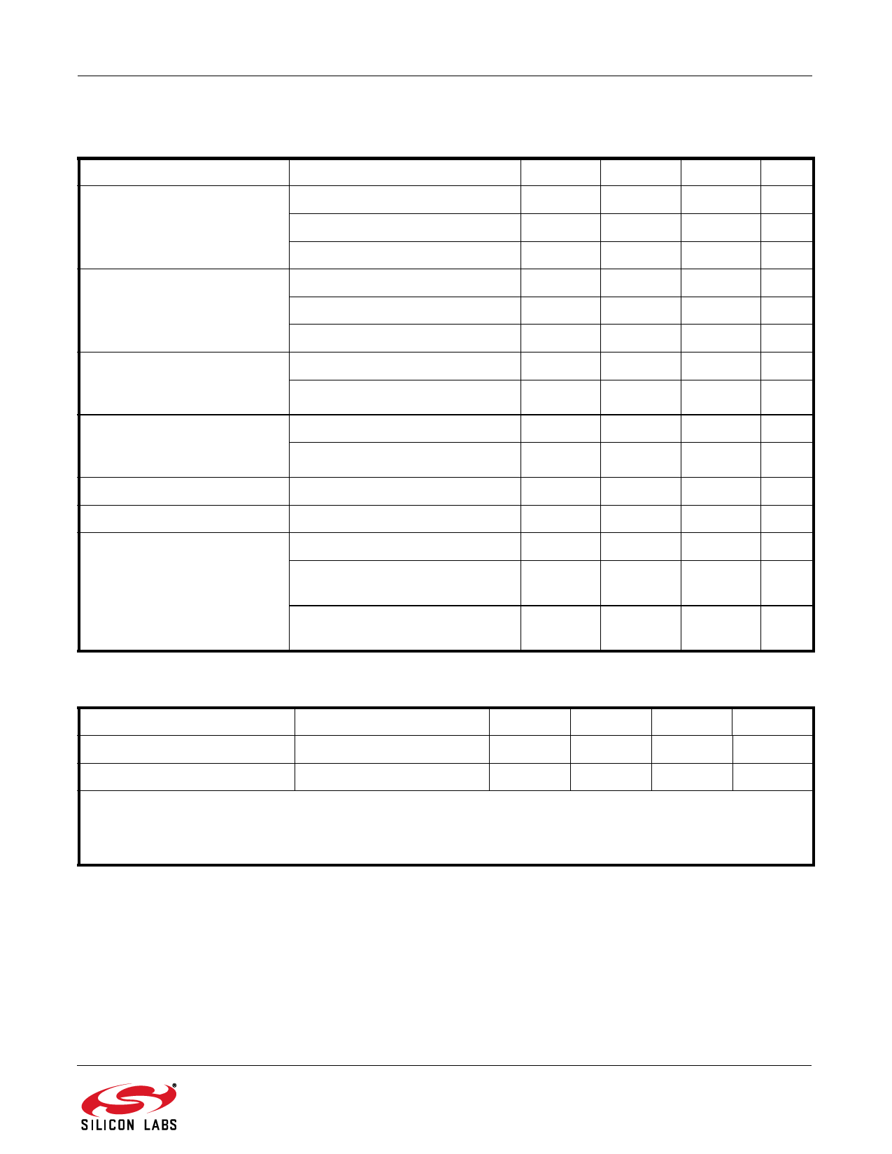
Table 1.3. Port I/O DC Electrical Characteristics
VDD = 1.8 to 3.6 V, –40 to +85 °C unless otherwise specified.
Parameter
Output High Voltage
(High Drive Strength,
PnDRV.n = 1)
Output High Voltage
(Low Drive Strength,
PnDRV.n = 0)
Output Low Voltage
(High Drive Strength,
PnDRV.n = 1)
Conditions
IOH = –3 mA, Port I/O push-pull
IOH = –10 µA
IOH = –10 mA
IOH = –1 mA
IOH = –10 µA
IOH = –3 mA
IOL = 8.5 mA
IOL = 25 mA
Output Low Voltage
(Low Drive Strength,
PnDRV.n = 0)
IOL = 1.4 mA
IOL = 4 mA
Input High Voltage
Input Low Voltage
Input Leakage Current
VDD = 2.0 to 3.6 V
VDD = 2.0 to 3.6 V
Weak Pull–up Off
Weak Pull-up On, VIN=0 V,
VDD = 1.8 V
Weak Pull-up On, VIN = 0 V,
VDD = 3.6 V
Min
Typ
VDD – 0.7
VDD – 0.1
—
—
—
see chart
VDD – 0.7
VDD – 0.1
—
—
—
see chart
—
—
—
see chart
—
—
—
see chart
VDD – 0.6
—
—
—
—
—
—
4
—
23
Max
—
—
—
—
—
—
0.7
—
0.7
—
—
0.6
0.5
—
—
Units
V
V
V
V
V
V
V
V
V
V
V
µA
µA
µA
Table 1.4. I2C Slave Electrical Characteristics
Parameter
VDD Range
Internal I2C pull-ups
Condition
Min
Typ
Max
units
Required to meet I2C spec
1.8
—
3.6
V
Required to meet I2C spec
—
6
—
k
Note: Stresses above those listed under “Absolute Maximum Ratings” may cause permanent damage to the device. This is a
stress rating only and functional operation of the devices at those or any other conditions above those indicated in the
operation listings of this specification is not implied. Exposure to maximum rating conditions for extended periods may
affect device reliability.
Rev 1.1
14
Share Link: 