2SJ537 View Datasheet(PDF) - Toshiba
Part Name
Description
Manufacturer
2SJ537 Datasheet PDF : 6 Pages
| |||
2SJ537
TOSHIBA Field Effect Transistor Silicon P Channel MOS Type (L2−π−MOSVI)
2SJ537
Chopper Regulator, DC−DC Converter and Motor Drive
Applications
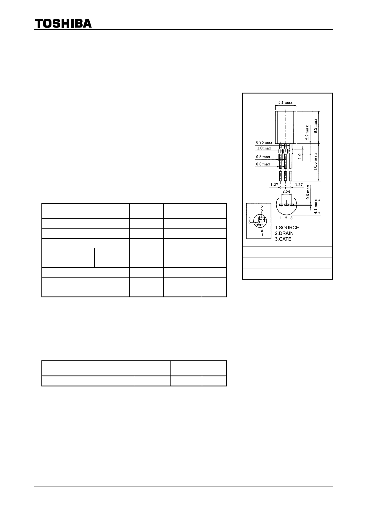
Unit: mm
z Low drain−source ON resistance
: RDS (ON) = 0.16 Ω (typ.)
z High forward transfer admittance
: |Yfs| = 3.5 S (typ.)
z Low leakage current : IDSS = −100 μA (VDS = −50 V)
z Enhancement mode : Vth = −0.8 to −2.0 V (VDS = −10 V, ID = −1 mA)
Absolute Maximum Ratings (Ta = 25°C)
Characteristics
Symbol
Rating
Unit
Drain−source voltage
Drain−gate voltage (RGS = 20 kΩ)
Gate−source voltage
Drain current
DC (Note 1)
Pulse (Note 1)
Drain power dissipation
Channel temperature
Storage temperature range
VDSS
VDGR
VGSS
ID
IDP
PD
Tch
Tstg
−50
V
−50
V
±20
V
−5
A
−15
A
0.9
W
150
°C
−55~150
°C
JEDEC
TO-92MOD
JEITA
―
TOSHIBA
2-5J1C
Weight: 0.36 g (typ.)
Note: Using continuously under heavy loads (e.g. the application of high temperature/current/voltage and the significant change in
temperature, etc.) may cause this product to decrease in the reliability significantly even if the operating conditions (i.e.
operating temperature/current/voltage, etc.) are within the absolute maximum ratings. Please design the appropriate
reliability upon reviewing the Toshiba Semiconductor Reliability Handbook (“Handling Precautions”/Derating Concept and
Methods) and individual reliability data (i.e. reliability test report and estimated failure rate, etc).
Thermal Characteristics
Characteristics
Symbol
Max
Unit
Thermal resistance, channel to ambient
Rth (ch−a)
138
°C / W
Note 1: Please use devices on condition that the channel temperature is below 150°C.
This transistor is an electrostatic sensitive device.
Please handle with caution.
1
2009-09-29
Share Link: 