LA70100M View Datasheet(PDF) - SANYO -> Panasonic
Part Name
Description
Manufacturer
LA70100M Datasheet PDF : 16 Pages
| |||
LA70100M
C.sync
VD
4.3MHz/1.1MHz
OSC
ENOSC
ENABLE
700µs
Fig.8 (b)
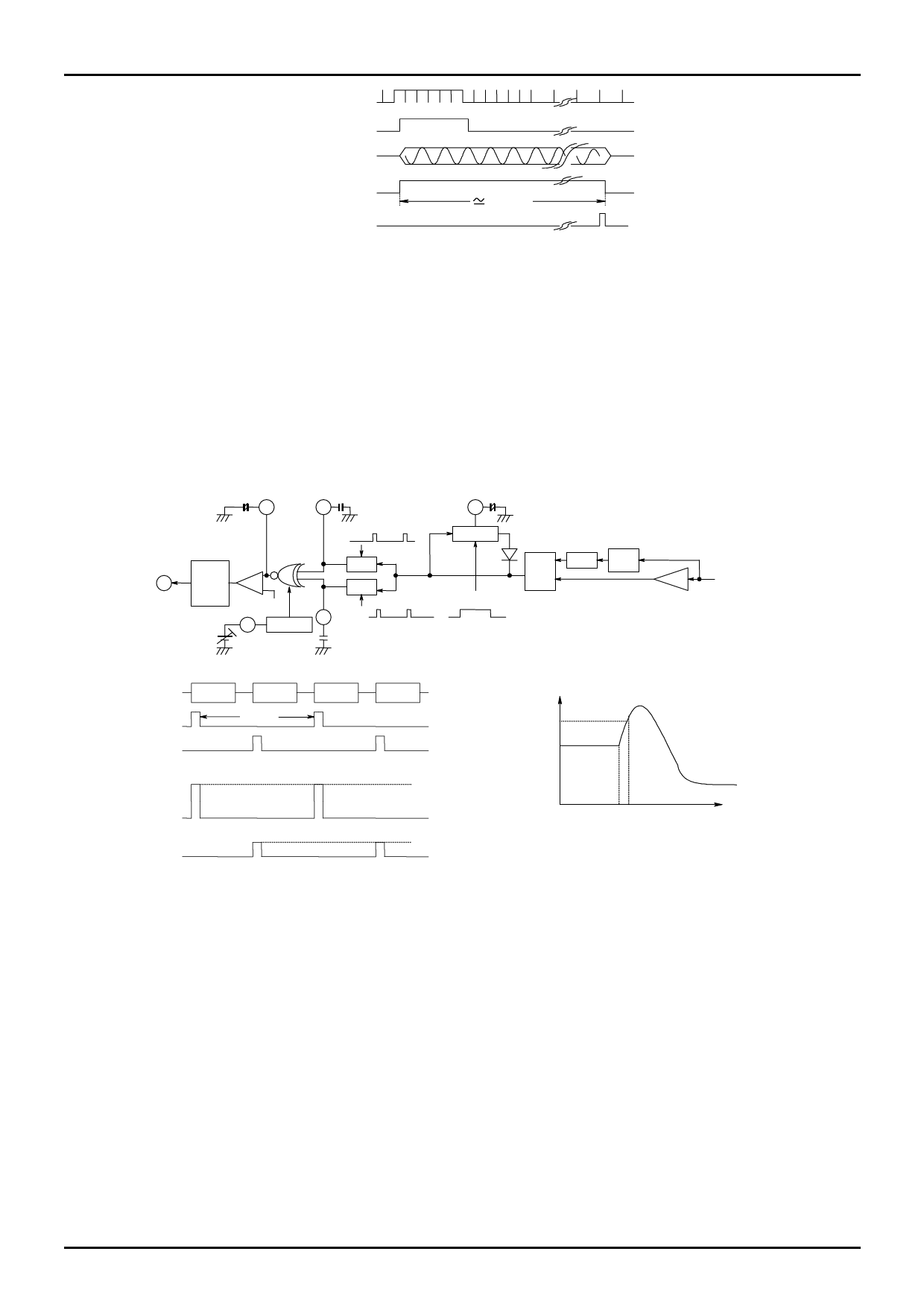
During a period when the color signal processing is left untouched (for about 700 µs from the start of vertical sync signal),
center frequency of BELL filter is automatically adjusted. MODE CONTROL sets each BELL/A-BELL filter into VCO mode
after vertical sync signal is input, then the OSC oscillates at 4.3MHz or 1.1MNz. Oscillation output is divided respectively by a
programmable divider and outputs the timing pulse that corresponds to oscillation frequency with control logic. This pulse is
compared with the timing pules acquired by dividing 4.43MHz CLK and generates UP or DOWN CLK corresponding to the
amount of discrepancies for oscillation frequency 4.286MHz/1.0715MHz. That is input to UP/DOWN counter to increase and
decrease the counter value. When ENABLE pulse is generated the outputs D0 to D5 are rewritten, and the control voltage
varies so that the oscillation frequency approach 4.286MHz/1.0715MHz. This operation repeats whenever the vertical sync
signal is input and stops when the frequency difference becomes to a specified value ( ±43kHz / ±10.7kHz ).
(9) SECAM
+ 27
25
DET S/H-1
S/H-3 21 +
SAMPLE HOLD PULSE
S/H-3
28 LOGIC COMP
SECAM DET OUT
Vref
SENS CONTROL
30 CTL
S/H-1
S/H-2
SAMPLE HOLD PULSE
26 S/H-2
PHASE
DET
BELL ADJUST PULSE
90 DEG
4.3MHz
BPF
Fig.9(a)
LIM
from MAIN SIGNAL LINE
Chroma
signal
SP1
SP2
SP3
VS1
VS2
128µs
Same as ESOSC at fig.8 (b)
V1
V2
Fig.9 (b)
Voltage
V2
VL
V1
4.25MHz 4.40625MHz Frequency
(4.28MHz)
Fig.9 (c)
The color signal with the amplitude limited by limiting circuit varies the phase according to the signal frequency after it
passes through a 4.3MHz BPF. DC voltage according to the phase can be acquired by shifting this output phase by further 90°
and inputting it to a phase detector with the original signal. The characteristic of the output of a phase detector is as shown in
the figure 9 (b), as the voltage limiting circuit operates at S/H-3 in order to prevent the malfunction caused by unwanted
signals. This limiting circuit voltage is the phase detector output DC voltage to which the signals of 4.286MHz VCO is input
used on BELL filter automatic adjusting circuit. Then it is possible to operate the limiting circuit exactly at a frequency more
than 4.286 MHz and to prevent the false discrimination during MESECAM signal input. After that, input to two sample & hold
circuits, the sampling pulse is shown like pulses correspond to BGP of NTSC and PAL generated every 1H as SP1 and SP2 in
figure 9 (b). The SECAM color signal has ID signals of 4.25MHz and 4.40625MHz generated every 1H on the part that
corresponds to this BGP, each phase detection output causes the level difference as V1, V2 in figure 9 (b). When this
difference is sampled by SP1 and SP2 the waveform becomes as VS1 and VS2 in the figure 9 (b), and when it is hold by
external capacitor it becomes as V1 and V2. Input to a comparator after detecting the difference of these two voltages,
smoothing it to stable with the external capacitor connected to Pin 27. In addition, applying more than 1V DC voltage to Pin
30 allows the amplification of the level difference to be varied.
When the smooth value of V1-V2 exceeds 3.5V, SECAM signal is detected with a high-level output from the Pin 28. This
discrimination circuit uses a rule that the output of a phase detector differs every 1H as shown in the figure 9 (b) (c) to detect a
SECAM signal. PAL signal always outputs high since its burst is constant and doesn’t vary phase detection output.
No.7204-10/16
Share Link: 