LH28F008SCL-12 View Datasheet(PDF) - Sharp Electronics
Part Name
Description
Manufacturer
LH28F008SCL-12 Datasheet PDF : 49 Pages
| |||
SHARI=
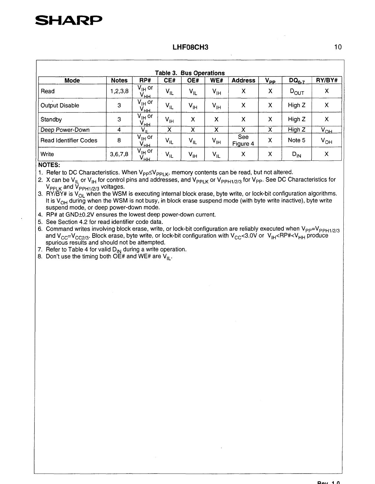
LHF08CH3
10
Mode
Notes
Table 3. Bus Operations
RP# CE# OE# WE# Address
VPP D&.-r
RY/BY#
Read
Output Disable
1,2,3,8 VT Or вҖңIL
вҖңIL
вҖңI,
HH
3
вҖңI, Or
Vr#
вҖңIL
вҖңI,
вҖҳ1,
X
X
DOUT
X
X
X
High Z
X
Standby
Deep Power-Down
Read Identifier Codes
3
вҖңI, Or
VHH
вҖңI,
X
X
X
X
High Z
X
4
V,,
X
X
X
X
X
High Z
Vn,,
8
вҖңI, Or
VHH
вҖңIL
вҖңIL
See
vlH
Figure 4 вҖҷ
Note 5
вҖңOH
Write
3,6,7,8 вҖң. Or вҖңIL
вҖңI,
вҖңIL
X
X
DlN
X
HH
вҖҳ4OTES:
I. Refer to DC Characteristics. When Vpp<VppLK, memory contents can be read, but not altered.
!. X can be VI, or VrH for control pins and addresses, and V,,,, or VPpHf/2/s for VP,. See DC Characteristics for
vPPLK and вҖңPPHl12i3
voltaw
3. RY/BY# is V,, when the WSM is executing internal block erase, byte write, or lock-bit configuration algorithms.
It is VOH during when the WSM is not busy, in block erase suspend mode (with byte write inactive), byte write
suspend mode, or deep power-down mode.
C. RP# at GNDk0.2вҖқ ensures the lowest deep power-down current.
i. See Section 4.2 for read identifier code data.
i. Command writes involving block erase, write, or lock-bit configuration are reliably executed when Vpp=VppH1/2/3
and vCC=vCC2/3.
Block erase, byte write, or lock-bit configuration with V,c<3.OV or VrH<RP#<VHH produce
spurious results and should not be attempted.
вҖҳ. Refer to Table 4 for valid DIN during a write operation.
1. DonвҖҷt use the timing both OE# and WE# are VI,.
Rev. 1 .O
Share Link: 