IS43TR16640A-125KBL View Datasheet(PDF) - Unspecified
Part Name
Description
Manufacturer
IS43TR16640A-125KBL Datasheet PDF : 71 Pages
| |||
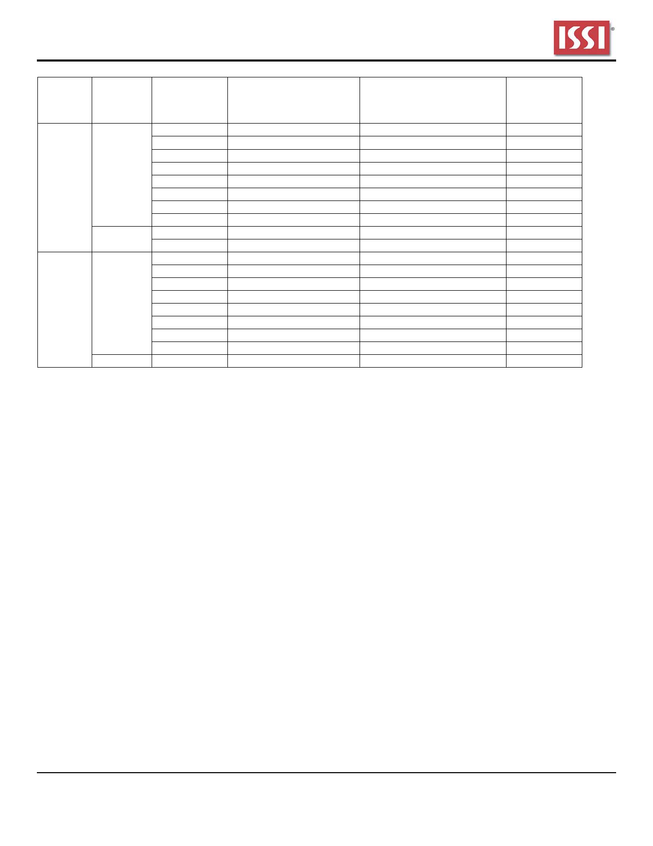
IS43TR16640A, IS43TR81280A
Burst
Length
READ/
WRITE
Starting
Column
ADDRESS
(A2,A1,A0)
burst type = Sequential
(decimal)
A3 = 0
burst type = Interleaved
(decimal)
A3 = 1
Notes
0
0,1,2,3,T,T,T,T
0,1,2,3,T,T,T,T
1, 2, 3
1
1,2,3,0,T,T,T,T
1,0,3,2,T,T,T,T
1, 2, 3
10
2,3,0,1,T,T,T,T
2,3,0,1,T,T,T,T
1, 2, 3
4
READ
11
100
3,0,1,2,T,T,T,T
4,5,6,7,T,T,T,T
Chop
101
5,6,7,4,T,T,T,T
3,2,1,0,T,T,T,T
4,5,6,7,T,T,T,T
5,4,7,6,T,T,T,T
1, 2, 3
1, 2, 3
1, 2, 3
110
6,7,4,5,T,T,T,T
6,7,4,5,T,T,T,T
1, 2, 3
111
7,4,5,6,T,T,T,T
7,6,5,4,T,T,T,T
1, 2, 3
WRITE
0,V,V
1,V,V
0,1,2,3,X,X,X,X
4,5,6,7,X,X,X,X
0,1,2,3,X,X,X,X
4,5,6,7,X,X,X,X
1, 2, 4, 5
1, 2, 4, 5
0
0,1,2,3,4,5,6,7
0,1,2,3,4,5,6,7
2
1
1,2,3,0,5,6,7,4
1,0,3,2,5,4,7,6
2
10
2,3,0,1,6,7,4,5
2,3,0,1,6,7,4,5
2
8
READ
11
100
3,0,1,2,7,4,5,6
4,5,6,7,0,1,2,3
3,2,1,0,7,6,5,4
4,5,6,7,0,1,2,3
2
2
101
5,6,7,4,1,2,3,0
5,4,7,6,1,0,3,2
2
110
6,7,4,5,2,3,0,1
6,7,4,5,2,3,0,1
2
111
7,4,5,6,3,0,1,2
7,6,5,4,3,2,1,0
2
WRITE
V,V,V
0,1,2,3,4,5,6,7
0,1,2,3,4,5,6,7
2, 4
Notes:
1. In case of burst length being fixed to 4 by MR0 setting, the internal write operation starts two clock cycles earlier than for the BL8 mode. This means
that the starting point for tWR and tWTR will be pulled in by two clocks. In case of burst length being selected on-the-fly via A12/BC#, the internal
write operation starts at the same point in time like a burst of 8 write operation. This means that during on-the-fly control, the starting point for tWR
and tWTR will not be pulled in by two clocks.
2. 0...7 bit number is value of CA[2:0] that causes this bit to be the first read during a burst.
3. T: Output driver for data and strobes are in high impedance.
4. V: a valid logic level (0 or 1), but respective buffer input ignores level on input pins.
5. X: Don’t Care.
2.3.2.2 CAS Latency
The CAS Latency is defined by MR0 (bits A9-A11) as shown in Figure 2.3.2. CAS Latency is the delay, in clock cycles,
between the internal Read command and the availability of the first bit of output data. DDR3 SDRAM does not support
any half-clock latencies. The overall Read Latency (RL) is defined as Additive Latency (AL) + CAS Latency (CL); RL = AL
+ CL. For more information on the supported CL and AL settings based on the operating clock frequency, refer to
“Standard Speed Bins”.
2.3.2.3 Test Mode
The normal operating mode is selected by MR0 (bit A7 = 0) and all other bits set to the desired values shown in Figure
2.3.2. Programming bit A7 to a ‘1’ places the DDR3 SDRAM into a test mode that is only used by the DRAM Manufacturer
and should NOT be used. No operations or functionality is specified if A7 = 1.
2.3.2.4 DLL Reset
The DLL Reset bit is self-clearing, meaning that it returns back to the value of ‘0’ after the DLL reset function has been
issued. Once the DLL is enabled, a subsequent DLL Reset should be applied. Any time that the DLL reset function is
used, tDLLK must be met before any functions that require the DLL can be used (i.e., Read commands or ODT
synchronous operations).
2.3.2.5 Write Recovery
The programmed WR value MR0 (bits A9, A10, and A11) is used for the auto precharge feature along with tRP to
determine tDAL. WR (write recovery for auto-precharge) min in clock cycles is calculated by dividing tWR (in ns) by tCK
(in ns) and rounding up to the next integer: WRmin[cycles] = Roundup(tWR[ns]/tCK[ns]). The WR must be programmed to
be equal to or larger than tWR(min).
Integrated Silicon Solution, Inc. – www.issi.com –
11
Rev. 00A
04/16/2012
Share Link: 