TC7136 View Datasheet(PDF) - Microchip Technology
Part Name
Description
Manufacturer
TC7136 Datasheet PDF : 22 Pages
| |||
TC7136/TC7136A
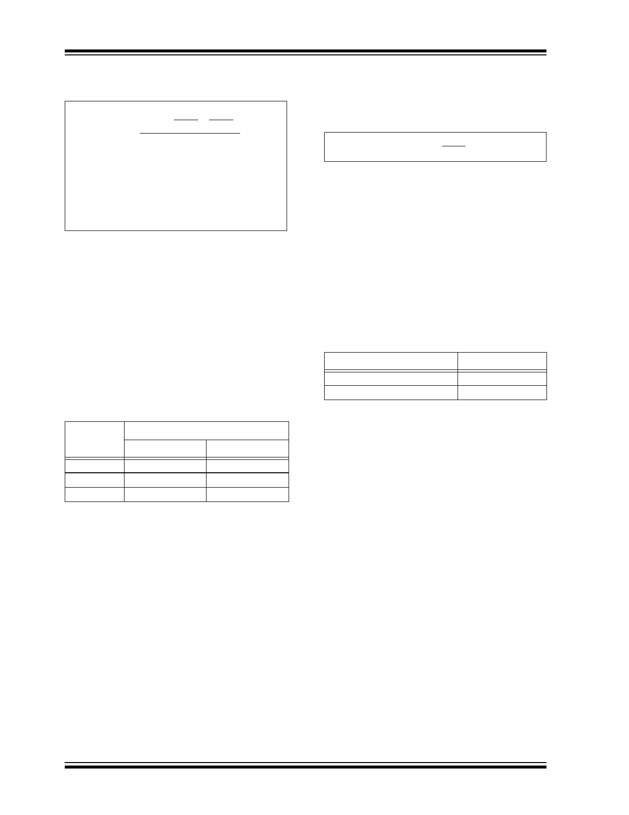
An exact expression for CINT is:
EQUATION 6-1:
(4000)⎛ 1 ⎞ ⎛ VFS ⎞
CINT =
⎝ FOSC ⎠ ⎝ RINT ⎠
VINT
Where:
FOSC = Clock frequency at Pin 38
VFS = Full scale input voltage
RINT = Integrating resistor
VINT = Desired full scale integrator output swing
CINT must have low dielectric absorption to minimize
rollover error. A polypropylene capacitor is
recommended.
6.4 Integrating Resistor (RINT)
The input buffer amplifier and integrator are designed
with Class A output stages. The output stage idling cur-
rent is 6μA. The integrator and buffer can supply 1μA
drive currents with negligible linearity errors. RINT is
chosen to remain in the output stage linear drive
region, but not so large that PC board leakage currents
induce errors. For a 200mV full scale, RINT is 180kΩ. A
2V full scale requires 1.8MΩ (see Table 6-1).
TABLE 6-1:
Component
Value
Nominal Full Scale Voltage
200mV
2V
CAZ
RINT
CINT
0.47μF
180kΩ
0.047μF
0.1μF
1.8MΩ
0.047μF
Note:
FOSC = 48kHz (3 reading per sec).
ROSC = 180kΩ, COSC = 50pF.
6.5 Oscillator Components
COSC should be 50pF. ROSC is selected from the
equation:
EQUATION 6-2:
FOSC =
0.45
RC
Note that FOSC is ÷ 4 to generate the TC7136A's inter-
nal clock. The backplane drive signal is derived by
dividing FOSC by 800.
To achieve maximum rejection of 60Hz noise pickup,
the signal integrate period should be a multiple of
60Hz. Oscillator frequencies of 240kHz, 120kHz,
80kHz, 60kHz, 40kHz, etc. should be selected. For
50Hz rejection, oscillator frequencies of 200kHz,
100kHz, 66-2/3kHz, 50kHz, 40kHz, etc. would be suit-
able. Note that 40kHz (2.5 readings per second) will
reject both 50Hz and 60Hz.
6.6 Reference Voltage Selection
A full scale reading (2000 counts) requires the input
signal be twice the reference voltage.
Required Full Scale Voltage*
200mV
2V
VREF
100mV
1V
Note: *VREF = 2VREF.
In some applications, a scale factor other than unity
may exist between a transducer output voltage and the
required digital reading. Assume, for example, a pres-
sure transducer output for 2000 lb/in2 is 400mV. Rather
than dividing the input voltage by two, the reference
voltage should be set to 200mV. This permits the trans-
ducer input to be used directly. The differential refer-
ence can also be used when a digital zero reading is
required, when VIN is not equal to zero. This is common
in temperature measuring instrumentation. A compen-
sating offset voltage can be applied between analog
common and VIN-. The transducer output is connected
between VIN+ and analog common.
DS21461C-page 12
© 2005 Microchip Technology Inc.
Share Link: 