TC7136 View Datasheet(PDF) - Microchip Technology
Part Name
Description
Manufacturer
TC7136 Datasheet PDF : 22 Pages
| |||
TC7136/TC7136A
7.0 DEVICE PIN FUNCTIONAL
DESCRIPTION
7.1 Differential Signal Inputs
VIN+ (Pin 31), VIN- (Pin 30)
The TC7136/A is designed with true differential inputs
and accepts input signals within the input stage Com-
mon mode voltage range (VCM). The typical range is
V+ – 1V to V- + 1V. Common mode voltages are
removed from the system when the TC7136A operates
from a battery or floating power source (isolated from
measured system), Common mode voltage removed
in battery operation with VIN = analog common and VIN-
is connected to analog common (VCOM) (see
Figure 7-1).
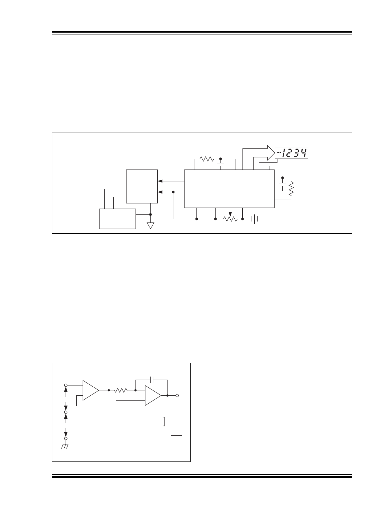
FIGURE 7-1:
COMMON MODE VOLTAGE REMOVED IN BATTERY OPERATION WITH
VIN = ANALOG COMMON
Segment
Drive
LCD
Measured
System
V+
V- GND
V+ V- GND
Power
Source
VBUF
CAZ VINT
V+
TC7136
V-
TC7136A
ANALOG
COMMON
VREF-
VREF+
V+
POL BP
OSC1
OSC3
OSC2
V-
+
9V
In systems where Common mode voltages exist, the
86dB Common mode rejection ratio minimizes error.
Common mode voltages do, however, affect the inte-
grator output level. A worst case condition exists if a
large positive VCM exists in conjunction with a full scale
negative differential signal. The negative signal drives
the integrator output positive along with VCM (see
Figure 7-2.) For such applications, the integrator out-
put swing can be reduced below the recommended 2V
full scale swing. The integrator output will swing within
0.3V of V+ or V- without increased linearity error.
FIGURE 7-2:
COMMON MODE
VOLTAGE REDUCES
AVAILABLE INTEGRATOR
SWING (VCOM ≠ VIN)
Input Buffer
CI
+
VIN
–
VCM
+
RI
–
–
+
VI
Integrator
[ VI
Where:
=
tI
CI
VCM = VIN
tI = Integration time
=
4000
FOSC
CI = Integration capacitor
RI = Integration resistor
7.2 Differential Reference
VREF+ (Pin 36), VREF- (Pin 35)
The reference voltage can be generated anywhere
within the V+ to V- power supply range.
To prevent rollover type errors being induced by large
Common mode voltages, CREF should be large com-
pared to stray node capacitance. The TC7136/A offers
a significantly improved analog common temperature
coefficient. This potential provides a very stable volt-
age, suitable for use as a voltage reference. The
temperature coefficient of analog common is typically
35ppm/°C.
7.3 Analog Common (Pin 32)
The analog common pin is set at a voltage potential
approximately 3V below V+. The potential is between
2.7V and 3.35V below V+. Analog common is tied inter-
nally to an N-channel FET, capable of sinking 100μA.
This FET will hold the common line at 3V below V+ if an
external load attempts to pull the common line toward
V+. Analog common source current is limited to 1μA.
Analog common is, therefore, easily pulled to a more
negative voltage (i.e., below V+ – 3V).
© 2005 Microchip Technology Inc.
DS21461C-page 13
Share Link: 