TC7136 View Datasheet(PDF) - Microchip Technology
Part Name
Description
Manufacturer
TC7136 Datasheet PDF : 22 Pages
| |||
TC7136/TC7136A
The TC7136/A connects the internal VIN+ and VIN-
inputs to analog common during the auto-zero phase.
During the reference integrate phase, VIN- is connected
to analog common. If VIN- is not externally connected to
analog common, a Common mode voltage exists, but
is rejected by the converter's 86dB Common mode
rejection ratio. In battery operation, analog common
and VIN- are usually connected, removing Common
mode voltage concerns. In systems where VIN- is con-
nected to the power supply ground or to a given
voltage, analog common should be connected to VIN-.
The analog common pin serves to set the analog sec-
tion reference, or common point. The TC7136A is spe-
cifically designed to operate from a battery, or in any
measurement system where input signals are not refer-
enced (float), with respect to the TC7136A power
source. The analog common potential of V+ – 3V gives
a 7V end of battery life voltage. The common potential
has a 0.001%/% voltage coefficient.
With sufficiently high total supply voltage
(V+ – V- > 7V), analog common is a very stable poten-
tial with excellent temperature stability (typically
35ppm/°C for TC7136A. This potential can be used to
generate the TC7136A's reference voltage. An external
voltage reference will be unnecessary in most cases,
because of the 35ppm/°C temperature coefficient. See
Section 7.5, TC7136A Internal Voltage Reference
discussion.
7.4 TEST (Pin 37)
The TEST pin potential is 5V less than V+. TEST may
be used as the negative power supply connection for
external CMOS logic. The TEST pin is tied to the inter-
nally generated negative logic supply through a 500Ω
resistor. The TEST pin load should not be more than
1mA. See Section 8.0, Typical Applications for addi-
tional information on using TEST as a negative digital
logic supply.
If TEST is pulled high (to V+), all segments plus the
minus sign will be activated. DO NOT OPERATE IN
THIS MODE FOR MORE THAN SEVERAL MINUTES.
With TEST = V+, the LCD segments are impressed with
a DC voltage which will destroy the LCD.
7.5 TC7136A Internal Voltage
Reference
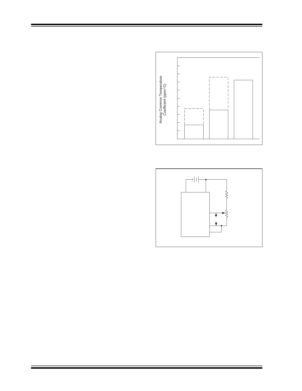
The TC7136 analog common voltage temperature sta-
bility has been significantly improved (Figure 7-3). The
"A" version of the industry standard TC7136 device
allows users to upgrade old systems and design new
systems without external voltage references. External
R and C values do not need to be changed; however,
noise performance will be improved by increasing CAZ
(see Section 6.1, Auto-Zero Capacitor). Figure 7-4
shows analog common supplying the necessary
voltage reference for the TC7136/A.
FIGURE 7-3:
ANALOG COMMON
TEMPERATURE
COEFFICIENT
200
180
160
Maximum No Maximum
Specified
140
Typical
120
100
80
Maximum
Typical
60
40
Typical
20
TC7136A
TC7136
ICL7136
0
FIGURE 7-4:
TC7136A INTERNAL
VOLTAGE REFERENCE
CONNECTION
9V
+
26
1
V-
V+
TC7136
TC7136A
VREF+ 36
VREF
VREF- 35
ANALOG 32
COMMON
Set VREF = 1/2 VREF
240kΩ
10kΩ
DS21461C-page 14
© 2005 Microchip Technology Inc.
Share Link: 