BU1425AK View Datasheet(PDF) - ROHM Semiconductor
Part Name
Description
Manufacturer
BU1425AK Datasheet PDF : 32 Pages
| |||
Multimedia ICs
BU1425AK / BU1425AKV
•Circuit operation
(1) Overview
The BU1425AK / AKV converts digital images and video
data with an 8-bit configuration to 9-bit composite signals
(VOUT), luminance signals (YOUT), and chrominance sig-
nals (COUT) for the NTSC, PAL, and PAL60 formats,
and outputs the converted data as analog TV signals.
The user may select whether VOUT consists of chromi-
nance signals that have passed through a chrominance
band pass and luminance signals that have been mixed,
or luminance signals that have passed through a chromi-
nance trap and luminance signals that have not passed
through a chrominance trap. The F characteristic of this
chrominance trap may be selected from among three
available types. Since YOUT normally does not pass
through the trap, it is optimum for the S pin. COUT nor-
mally passes through the chrominance band pass, and is
thus highly resistance to dot interference. In addition,
when used in the doubled clock mode, it passes through
an interpolator filter, and for that reason is able to repro-
duce even cleaner image quality.
A correspondence can be set up between input digital
image data and Video-CD and CD-G decoder output.
Output TV signals, in addition to switching among the
NTSC, PAL, and PAL60 modes, can be switched
between the interlace and non-interlace modes.
The data clock input to the VCLK pin can also be input as
a doubled clock for the data rate (in doubled clock
modes). In doubled clock modes, data is read and
processed at the rising edge of an internal clock that has
been divided in half. In ordinary clock modes, data is
read and processed at the rising edge of the clock that
has the same phase as the input clock. Two input data
formats are supported: 24-bit RGB (4: 4: 4) and 16-bit
YUV (4: 2: 2). These are input to RD0 to 7, GD0 to 7, and
BD0 to 7, respectively. The selected input format can be
switched using the IM0 and IM1 pin input. When the
OSDSW pin is set to the "Enabled" (H) state, data input
to the ROSD, GOSD, and BOSD pins becomes effective,
making it possible to input 7-color (8 including black)
chrominance data. At the same time, a clock with a fre-
quency half that of the internal clock is output from the
PIXCLK pin. As a result, the PIXCLK pin can easily be
directly connected to the OSD IC clock input pin, and the
OSDSW pin can be directly connected to the BLK output
pin. Thus, the BU1425AK and the OSD IC can be syn-
chronized, and OSD text with a burster trimmer stacker
feature can be used.
If the input data is in the RGB format, it is converted to
YUV. If it is in the YUV format, it is converted from the
CCIR-601 format to level-shifted YUV data. The YUV
data is then adjusted to the 100IRE level in the NTSC,
PAL, and PAL60 modes, and U and V data is phase-
adjusted by a sub-carrier generated internally, and is
modulated to chrominance signals.
Ultimately, elements such as the necessary synchroniza-
tion level, the color blanking level, and burst signals are
mixed, and pass through the 9-bit DAC to be output as
NTSC or PAL composite signals, luminance signals, and
chrominance signals (conforming to RS-170A). At this
point, the DAC is operating at twice the internal clock,
making it possible to reduce the number of attachments.
Furthermore, luminance signal output and chrominance
signal output can be turned off. At this point, it is possible
to reduce the level of power consumption.
The DAC output is current output. If a resistor of a speci-
fied value is connected to the IR pin, 2.0VP-P output can
be obtained by connecting 75Ω to the VOUT pin as an
external resistor. As a result, normally, when a video
input pin (75Ω terminus) is connected, the output is
approximately 1.0VP-P voltage output at a white 100%
level.
(2) Specifying the mode
1) Power saving mode
With the BU1425AK / AKV, setting the YCOFF pin to
HIGH turns off the output from the YOUT and COUT pins
of the DAC output, enabling use in the low power con-
sumption mode.
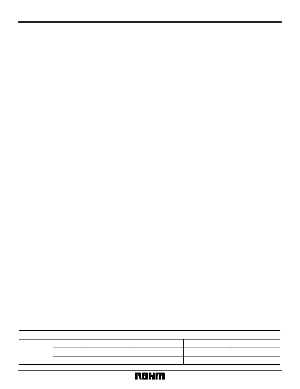
Table 1: Low power consumption mode with the YCOFF pin
Pin No.
48
Pin Name
YCOFF
LOW
HIGH
VOUT pin
Composite signal
Composite signal
Output Mode and Power Consumption
YOUT pin
COUT pin
Power consumption (typ.)
Luminance signal Chrominance signal
0.45W
No output (0V)
No output (0V)
0.25W
11
Share Link: 