S25FL016A View Datasheet(PDF) - Spansion Inc.
Part Name
Description
Manufacturer
S25FL016A
Spansion Inc.

S25FL016A Datasheet PDF : 36 Pages
| |||
Data Sheet
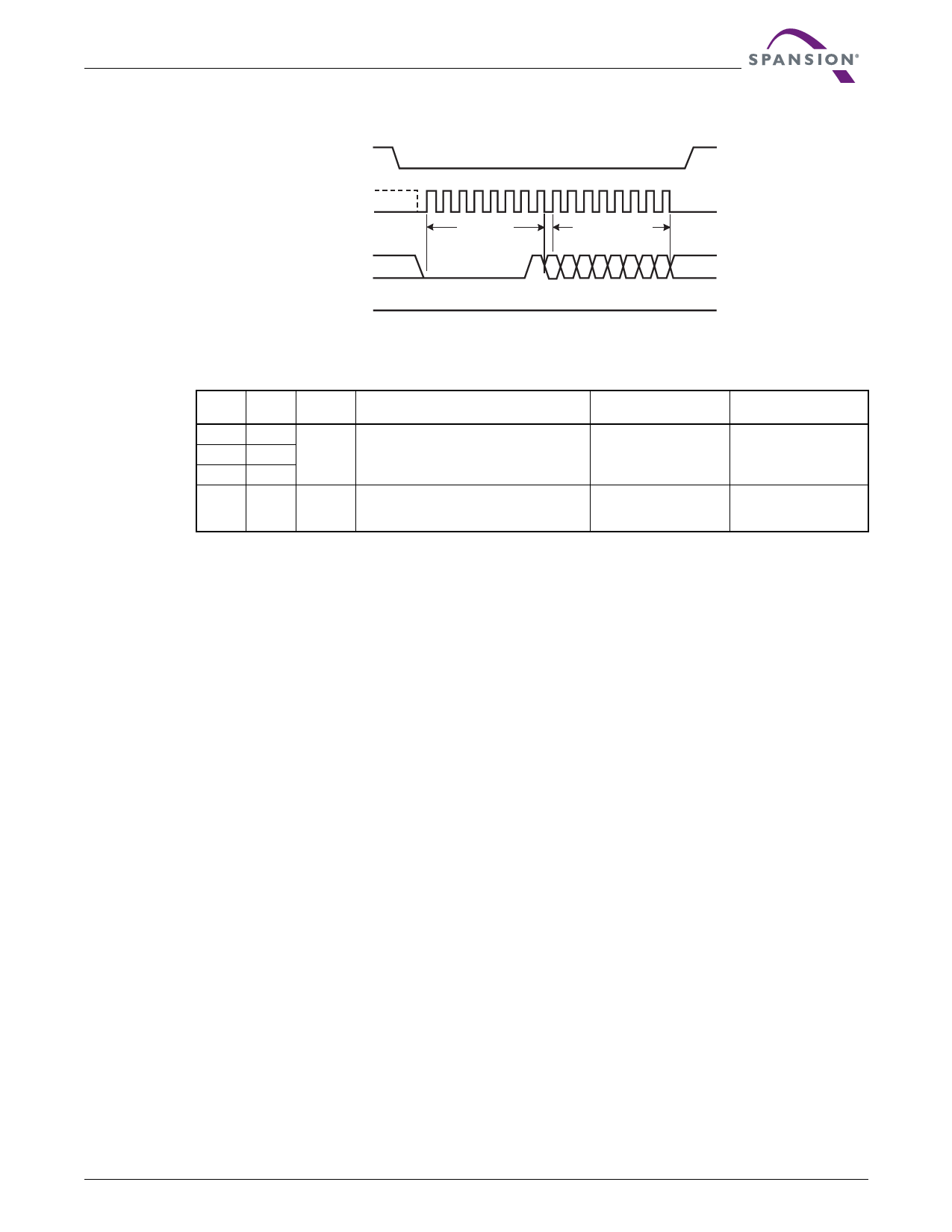
Figure 9.7 Write Status Register (WRSR) Command Sequence
CS#
Mode 3
SCK Mode 0
0 1 2 3 4 5 6 7 8 9 10 11 12 13 14 15
Command
Status Register In
SI
Hi-Z
SO
76543210
MSB
9.8
Table 9.3 Protection Modes
W# SRWD
Signal Bit
Mode
Write Protection of the Status Register
Protected Area
(See Note)
Unprotected Area
(See Note)
1
1
0
1
0
0
Software
Protected
(SPM)
Status Register is writable (if the WREN
command has set the WEL bit). The values in
the SRWD, BP2, BP1 and BP0 bits can be
changed.
Protected against program
and erase commands
Ready to accept Page
Program and Sector Erase
commands
0
1
Hardware Status Register is Hardware write protected.
Protected The values in the SRWD, BP2, BP1 and BP0
(HPM)
bits cannot be changed.
Protected against program
and erase commands
Ready to accept Page
Program and Sector Erase
commands
Note
As defined by the values in the Block Protect (BP2, BP1, BP0) bits of the Status Register, as shown in Table 7.1 on page 13.
Table 9.3 shows that neither W# or SRWD bit by themselves can enable HPM. The device can enter HPM
either by setting the SRWD bit after driving W# low, or by driving W# low after setting the SRWD bit.
However, the device disables HPM only when W# is driven high.
Note that HPM only protects against changes to the status register. Since BP2:BP0 cannot be changed in
HPM, the size of the protected area of the memory array cannot be changed. Note that HPM provides no
protection to the memory array area outside that specified by BP2:BP0 (Software Protected Mode, or SPM).
If W# is permanently tied high, HPM can never be activated, and only the SPM (BP2:BP0 bits of the Status
Register) can be used.
Page Program (PP)
The Page Program (PP) command changes specified bytes in the memory array (from 1 to 0 only). A WREN
command is required prior to writing the PP command.
The host system must drive CS# low, and then write the PP command, three address bytes, and at least one
data byte on SI. CS# must be driven low for the entire duration of the PP sequence. The command sequence
is shown in Figure 9.8 and Table 9.4 on page 25.
The device programs only the last 256 data bytes sent to the device. If the number of data bytes exceeds this
limit, the bytes sent before the last 256 bytes are discarded, and the device begins programming the last 256
bytes sent at the starting address of the specified page. This may result in data being programmed into
different addresses within the same page than expected. If fewer than 256 data bytes are sent to device, they
are correctly programmed at the requested addresses.
The host system must drive CS# high after the device has latched the 8th bit of the data byte, otherwise the
device does not execute the PP command. The PP operation begins as soon as CS# is driven high. The
device internally controls the timing of the operation, which requires a period of tPP. The Status Register may
be read to check the value of the Write In Progress (WIP) bit while the PP operation is in progress. The WIP
bit is 1 during the PP operation, and is 0 when the operation is completed. The device internally resets the
Write Enable Latch to 0 before the operation completes (the exact timing is not specified).
The device does not execute a Page Program (PP) command that specifies a page that is protected by the
Block Protect bits (BP2:BP0) (see Table 7.1 on page 13).
January 7, 2008 S25FL016A_00_C3
S25FL016A
21
Share Link: