56F8357 View Datasheet(PDF) - Motorola => Freescale
Part Name
Description
Manufacturer
56F8357 Datasheet PDF : 160 Pages
| |||
Freescale Semiconductor, Inc.
56F8357 Signal Pins
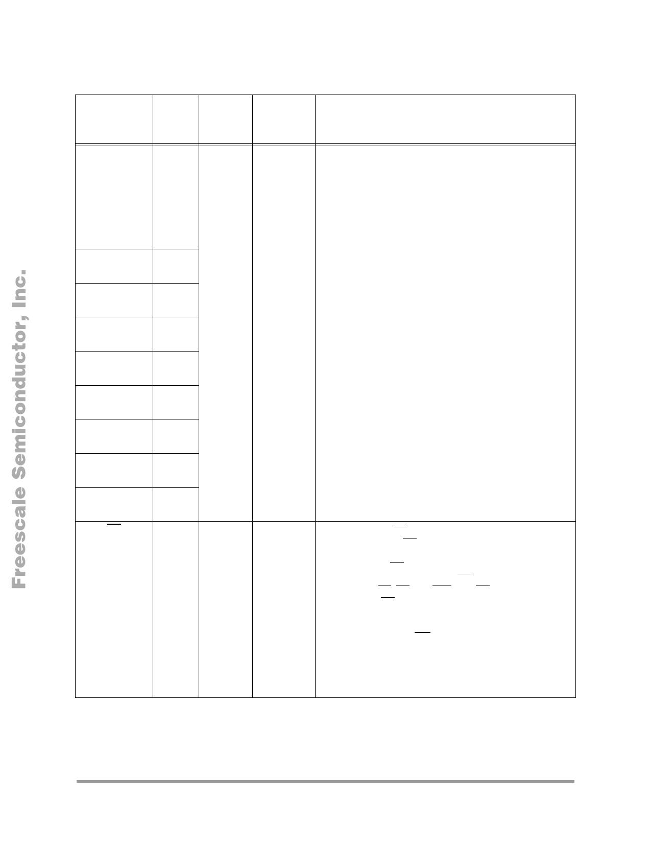
Table 2-2 56F8357 Signal and Package Information for the 160-Pin LQFP
Signal Name Pin No. Type
State
During
Reset
Signal Description
D7
(GPIOF0)
D8
(GPIOF1)
D9
(GPIOF2)
D10
(GPIOF3)
D11
(GPIOF4)
D12
(GPIOF5)
D13
(GPIOF6)
D14
(GPIOF7)
D15
(GPIOF8)
RD
28
Input/
Tri-stated Data Bus — D7 - D14 specify part of the data for external
Output
program or data memory accesses.
Depending upon the state of the DRV bit in the EMI bus
control register (BCR), D7 - D15and EMI control signals are
tri-stated when the external bus is inactive.
Input/
Output
29
30
32
Input
Port F GPIO — These eight GPIO pins can be individually
programmed as input or output pins.
At reset, these pins default to data bus functionality.
To deactivate the internal pull-up resistor, clear the
appropriate GPIO bit in the GPIOF_PUR register.
Example: GPIOF0, clear bit 0 in the GPIOF_PUR register.
149
150
151
152
153
52
Output Tri-stated Read Enable — RD is asserted during external memory
read cycles. When RD is asserted low, pins D0 - D15
become inputs and an external device is enabled onto the
data bus. When RD is deasserted high, the external data is
latched inside the device. When RD is asserted, it qualifies
the A0 - A23, PS, DS, and CSn pins. RD can be connected
directly to the OE pin of a static RAM or ROM.
Depending upon the state of the DRV bit in the EMI bus
control register (BCR), RD is tri-stated when the external bus
is inactive.
To deactivate the internal pull-up resistor, set the CTRL bit
in the SIM_PUDR register.
56F8357 Technical Data
19
Preliminary
For More Information On This Product,
Go to: www.freescale.com
Share Link: 