LS7166 View Datasheet(PDF) - LSI Corporation
Part Name
Description
Manufacturer
LS7166 Datasheet PDF : 15 Pages
| |||
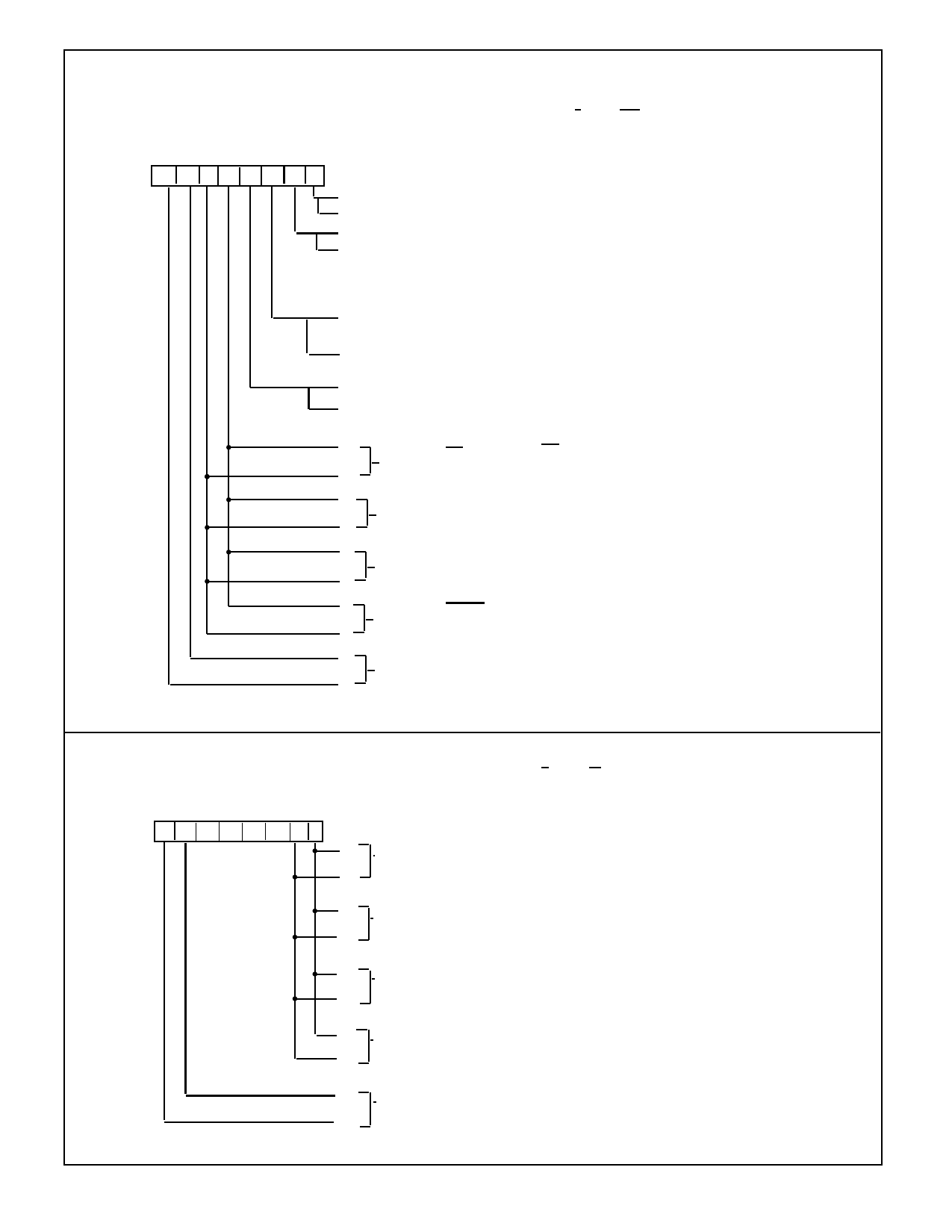
OCCR (Output Control Register) Initializes CNTR and output operating modes.
Accessed by : WRITE when C/D = 1, CS = 0.
Bit #
76543210
10
0: Binary count mode (Overridden by D3 = 1).
1: BCD count mode (Overridden by D3 = 1)
0: Normal count mode
1: Non-Recycle count mode. (CNTR enabled with a Load or Reset
CNTR and disabled with generation of Carry or Borrow.
In this mode no external CY or BW is generated. Instead
CYT or BWT should be used as cycle completion indicator.)
0: Normal count mode
1: Divide by N count mode (CNTR is reloaded with PR data upon
Carry or Borrow).
0: Binary or BCD count mode (see D0)
1: 24 Hour Clock mode with Byte 0 = Sec, Byte 1 = Min and Byte 2 = Hr.
(Overrides BCD/Binary Modes)
0 Pin 16 = CY, Pin 17 = BW. (Active Low)
0
1 Pin 16 = CYT, Pin 17 = BWT
0
0 Pin 16 = CY, Pin 17 = BW. (Active high)
1
1 Pin 16 = COMP, Pin 17 = COMPT
1
0 Select OCCR
1
QR (Quadrature Register). Selects quadrature count mode (See Fig. 7)
Accessed by: WRITE when C/D = 1, CS = 0.
Bit # 7 6 5 4 3 2 1 0
11XXXX
0
0
Disable quadrature mode
1 Enable x1 quadrature mode
0
0 Enable x2 quadrature mode
1
1 Enable x4 quadrature mode
1
7166-110103-4
X = Don’t Care
1 Select QR
1
Share Link: 