MPC2104 View Datasheet(PDF) - Motorola => Freescale
Part Name
Description
Manufacturer
MPC2104
Motorola => Freescale

MPC2104 Datasheet PDF : 24 Pages
| |||
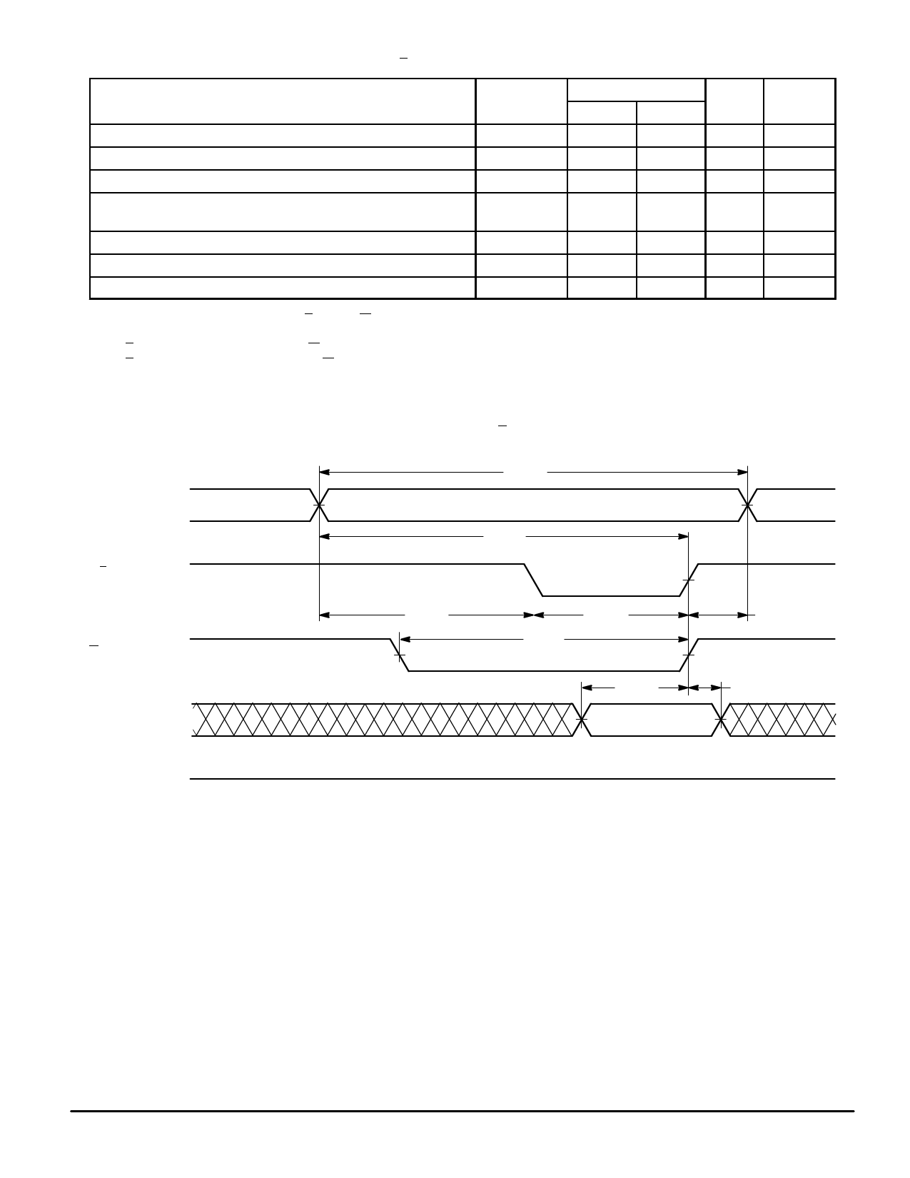
ASYNCHRONOUS DATA RAMs WRITE CYCLE 2 (E Controlled, See Notes 1 and 2)
MPC2107–15
Parameter
Symbol
Min
Max
Write Cycle Time
Address Setup Time
Address Valid to End of Write
Enable to End of Write
tAVAV
15
—
tAVEL
0
—
tAVEH
12
—
tELEH
10
—
tELWH
Data Valid to End of Write
tDVEH
7
—
Data Hold Time
tEHDX
0
—
Write Recovery Time
tEHAX
0
—
NOTES:
1. A write occurs during the overlap of E low and W low.
2. All timings are referenced from the last valid address to the first transitioning address.
3. If E goes low coincident with or after W goes low, the output will remain in a high impedance state.
4. If E goes high coincident with or before W goes high, the output will remain in a high impedance state.
Unit
Notes
ns
0
ns
ns
ns
3, 4
ns
ns
ns
A (ADDRESS)
E (CHIP ENABLE)
W (WRITE ENABLE)
D (DATA IN)
Q (DATA OUT)
ASYNCHRONOUS WRITE CYCLE 2 (E Controlled, See Note 1)
tAVAV
tAVEH
tAVEL
tWLEH
tELEH
tELWH
tDVEH
DATA VALID
HIGH–Z
tEHAX
tEHDX
MOTOROLA FAST SRAM
MPC2104•MPC2105•MPC2106•MPC2107
15
Share Link: