PC8240 View Datasheet(PDF) - Atmel Corporation
Part Name
Description
Manufacturer
PC8240 Datasheet PDF : 42 Pages
| |||
PC8240
Table 9. Clock AC Timing Specifications (Continued)
Num Characteristics and Conditions(1)
Min
Max
Unit Notes
18 OSC_IN Cycle Time
40
15
ns
19 OSC_IN Rise and Fall Times
–
5
ns
(5)
20 OSC_IN Duty Cycle Measured at 1.4V
40
60
%
21 OSC_IN Frequency Stability
–
100
ppm
22
23
Notes:
OSC_IN VIH (Loaded)
TBD
V
OSC_IN VIL (Loaded)
–
TBD
V
1. These specifications are for the default driver strengths indicated in Table 7 on page 17.
2. Rise and fall times for the PCI_SYNC_IN input are measured from 0.4 to 2.4V.
3. Specification value at maximum frequency of operation.
4. Relock time is guaranteed by design and characterization. Relock time is not tested.
5. Rise and fall times for the OSC_IN input is guaranteed by design and characterization. OSC_IN input rise and fall times are
not tested.
6. Relock timing is guaranteed by design. PLL-relock time is the maximum amount of time required for PLL lock after a stable
Vdd and PCI_SYNC_IN are reached during the reset sequence. This specification also applies when the PLL has been dis-
abled and subsequently re-enabled during sleep mode. Also note that HRST_CPU/HRST_CTRL must be held asserted for
a minimum of 255 bus clocks after the PLL-relock time during the reset sequence.
7. DLL_EXTEND is bit 7 of the PMC2 register <72>. N is a non-zero integer (1, 2, 3, ...). Tclk is the period of one
SDRAM_SYNC_OUT clock cycle in ns. tloop is the propagation delay of the DLL synchronization feedback loop (PC board
runner) from SDRAM_SYNC_OUT to SDRAM_SYNC_IN in ns; 6.25 inches of loop length (unloaded PC board runner) cor-
responds to approximately 1 ns of delay. tfix0 is a fixed delay inherent in the design when the DLL is at tap point 0 and the
DLL is contributing no delay; tfix0 equals approximately 3 ns. See Figure 9 on page 20 for DLL locking ranges.
8. Pin to pin skew includes quantifying the additional amount of clock skew (or jitter) from the DLL besides any intentional skew
added to the clocking signals from the variable length DLL synchronization feedback loop, i.e. the amount of variance
between the internal sys-logic_clk and the SDRAM_SYNC_IN signal after the DLL is locked. While pin to pin skew between
SDRAM_CLKs can be measured, the relationship between the internal sys-logic_clk and the external SDRAM_SYNC_IN
cannot be measured and is guaranteed by design.
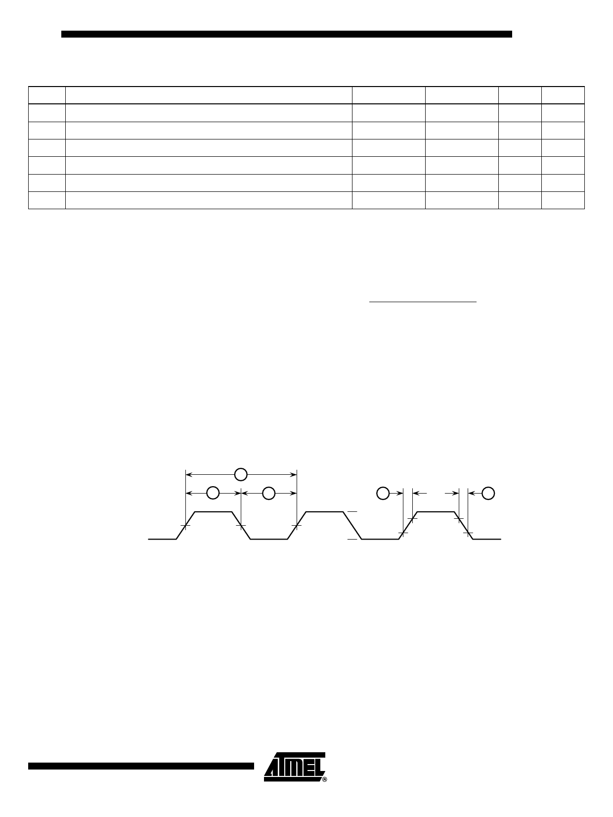
Figure 8. PCI_SYNC-IN Input Clock Timing Diagram
1
5a
5b
2
3
CVIL
PCI_SYNC_IN VM
VM
VM
CVIH
VM = Midpoint Voltage (1.4V)
19
2149A–HIREL–05/02
Share Link: 