LPC4357FET256 View Datasheet(PDF) - NXP Semiconductors.
Part Name
Description
Manufacturer
LPC4357FET256
NXP Semiconductors.

LPC4357FET256 Datasheet PDF : 162 Pages
| |||
NXP Semiconductors
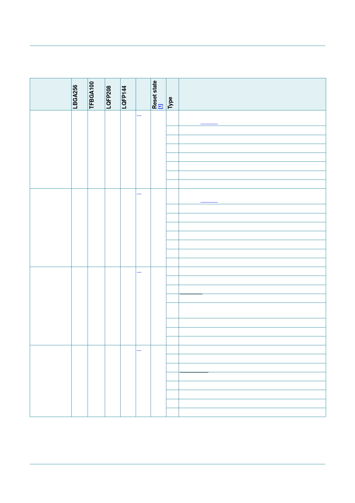
Table 3. Pin description …continued
Pin name
LPC435x/3x/2x/1x
32-bit ARM Cortex-M4/M0 microcontroller
Description
P1_1
P1_2
P1_3
P1_4
R2 K2 58 42 [2] N; I/O GPIO0[8] — General purpose digital input/output pin. Boot
PU
pin (see Table 5).
O CTOUT_7 — SCT output 7. Match output 3 of timer 1.
I/O EMC_A6 — External memory address line 6.
I/O SGPIO8 — General purpose digital input/output pin.
- R — Function reserved.
I/O SSP0_MISO — Master In Slave Out for SSP0.
- R — Function reserved.
I/O EMC_D13 — External memory data line 13.
R3 K1 60 43 [2] N; I/O GPIO0[9] — General purpose digital input/output pin. Boot
PU
pin (see Table 5).
O CTOUT_6 — SCT output 6. Match output 2 of timer 1.
I/O EMC_A7 — External memory address line 7.
I/O SGPIO9 — General purpose digital input/output pin.
- R — Function reserved.
I/O SSP0_MOSI — Master Out Slave in for SSP0.
- R — Function reserved.
I/O EMC_D14 — External memory data line 14.
P5 J1
61 44 [2]
N; I/O GPIO0[10] — General purpose digital input/output pin.
PU O CTOUT_8 — SCT output 8. Match output 0 of timer 2.
I/O SGPIO10 — General purpose digital input/output pin.
O EMC_OE — LOW active Output Enable signal.
O USB0_IND1 — USB0 port indicator LED control
output 1.
I/O SSP1_MISO — Master In Slave Out for SSP1.
- R — Function reserved.
O SD_RST — SD/MMC reset signal for MMC4.4 card.
T3 J2
64 47 [2]
N; I/O GPIO0[11] — General purpose digital input/output pin.
PU O CTOUT_9 — SCT output 9. Match output 3 of timer 3.
I/O SGPIO11 — General purpose digital input/output pin.
O EMC_BLS0 — LOW active Byte Lane select signal 0.
O USB0_IND0 — USB0 port indicator LED control output 0.
I/O SSP1_MOSI — Master Out Slave in for SSP1.
I/O EMC_D15 — External memory data line 15.
O SD_VOLT1 — SD/MMC bus voltage select output 1.
LPC435X_3X_2X_1X
Product data sheet
All information provided in this document is subject to legal disclaimers.
Rev. 5.2 — 26 November 2015
© NXP Semiconductors N.V. 2015. All rights reserved.
11 of 162
Share Link: