S25FL256SDSBFIQ01 View Datasheet(PDF) - Cypress Semiconductor
Part Name
Description
Manufacturer
S25FL256SDSBFIQ01
Cypress Semiconductor

S25FL256SDSBFIQ01 Datasheet PDF : 144 Pages
| |||
S25FL128S, S25FL256S
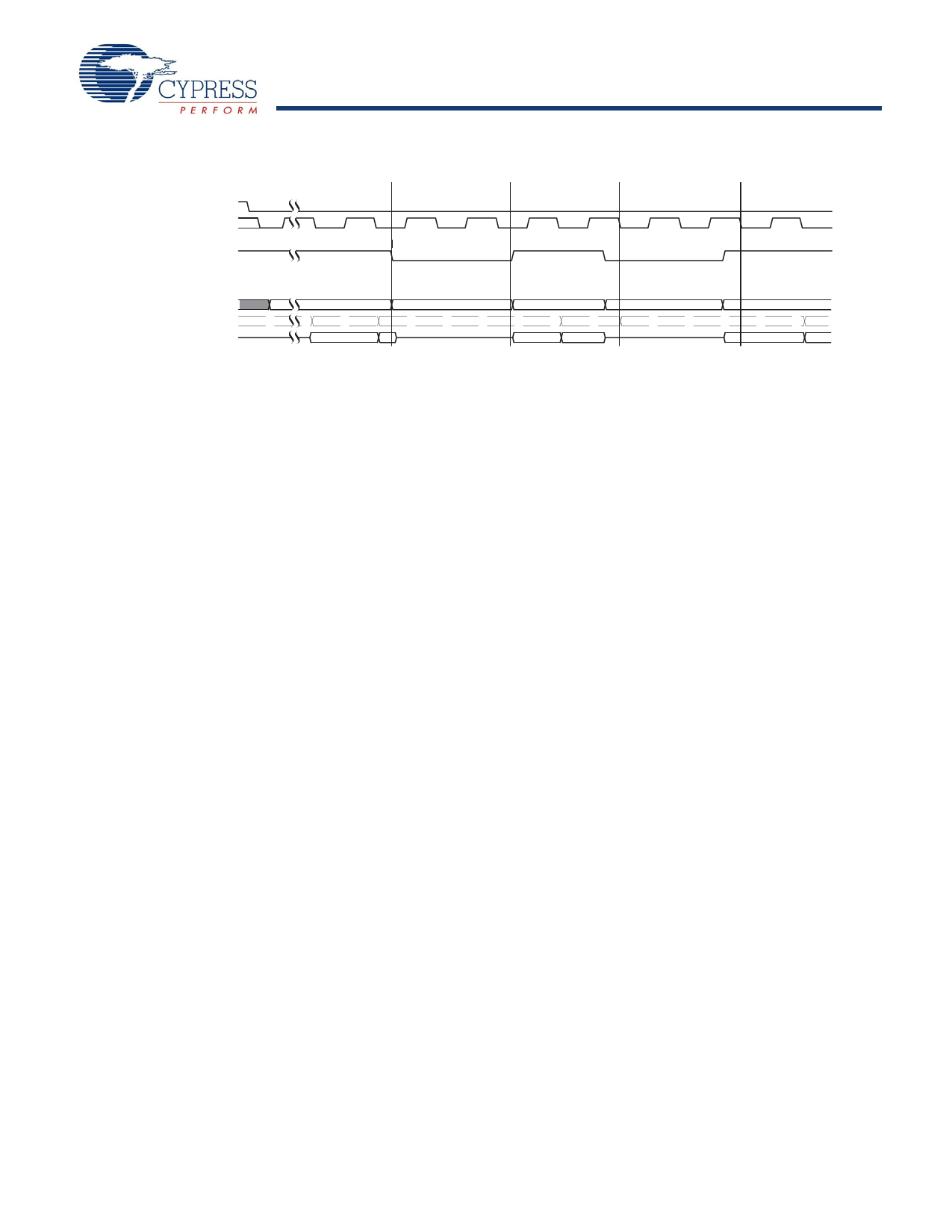
Figure 2.1 HOLD Mode Operation
CS#
SCK
HOLD#
SI_or_IO_(during_input)
SO_or_IO_(internal)
SO_or_IO_(external)
Valid Input
A
A
Hold Condition
Standard Use
Don't Care
B
B
Valid Input
C
B
C
Hold Condition
Non-standard Use
Don't Care
D
Valid Input
E
D
E
2.10 Core Voltage Supply (VCC)
VCC is the voltage source for all device internal logic. It is the single voltage used for all device internal functions including read,
program, and erase. The voltage may vary from 2.7V to 3.6V.
2.11 Versatile I/O Power Supply (VIO)
The Versatile I/O (VIO) supply is the voltage source for all device input receivers and output drivers and allows the host system to set
the voltage levels that the device tolerates on all inputs and drives on outputs (address, control, and IO signals). The VIO range is
1.65V to VCC. VIO cannot be greater than VCC.
For example, a VIO of 1.65V - 3.6V allows for I/O at the 1.8V, 2.5V or 3V levels, driving and receiving signals to and from other 1.8V,
2.5V or 3V devices on the same data bus. VIO may be tied to VCC so that interface signals operate at the same voltage as the core
of the device. VIO is not available in all package options, when not available the VIO supply is tied to VCC internal to the package.
During the rise of power supplies the VIO supply voltage must remain less than or equal to the VCC supply voltage. This supply is not
available in all package options. For a backward compatible SO16 footprint, the VIO supply is tied to VCC inside the package; thus,
the IO will function at VCC level.
2.12 Supply and Signal Ground (VSS)
VSS is the common voltage drain and ground reference for the device core, input signal receivers, and output drivers.
2.13 Not Connected (NC)
No device internal signal is connected to the package connector nor is there any future plan to use the connector for a signal. The
connection may safely be used for routing space for a signal on a Printed Circuit Board (PCB). However, any signal connected to an
NC must not have voltage levels higher than VIO.
2.14 Reserved for Future Use (RFU)
No device internal signal is currently connected to the package connector but is there potential future use of the connector. It is
recommended to not use RFU connectors for PCB routing channels so that the PCB may take advantage of future enhanced
features in compatible footprint devices.
2.15 Do Not Use (DNU)
A device internal signal may be connected to the package connector. The connection may be used by Cypress for test or other
purposes and is not intended for connection to any host system signal. Any DNU signal related function will be inactive when the
signal is at VIL. The signal has an internal pull-down resistor and may be left unconnected in the host system or may be tied to VSS.
Do not use these connections for PCB signal routing channels. Do not connect any host system signal to these connections.
Document Number: 001-98283 Rev. *I
Page 12 of 144
Share Link: