S25FL256SDSBFIQ01 View Datasheet(PDF) - Cypress Semiconductor
Part Name
Description
Manufacturer
S25FL256SDSBFIQ01
Cypress Semiconductor

S25FL256SDSBFIQ01 Datasheet PDF : 144 Pages
| |||
S25FL128S, S25FL256S
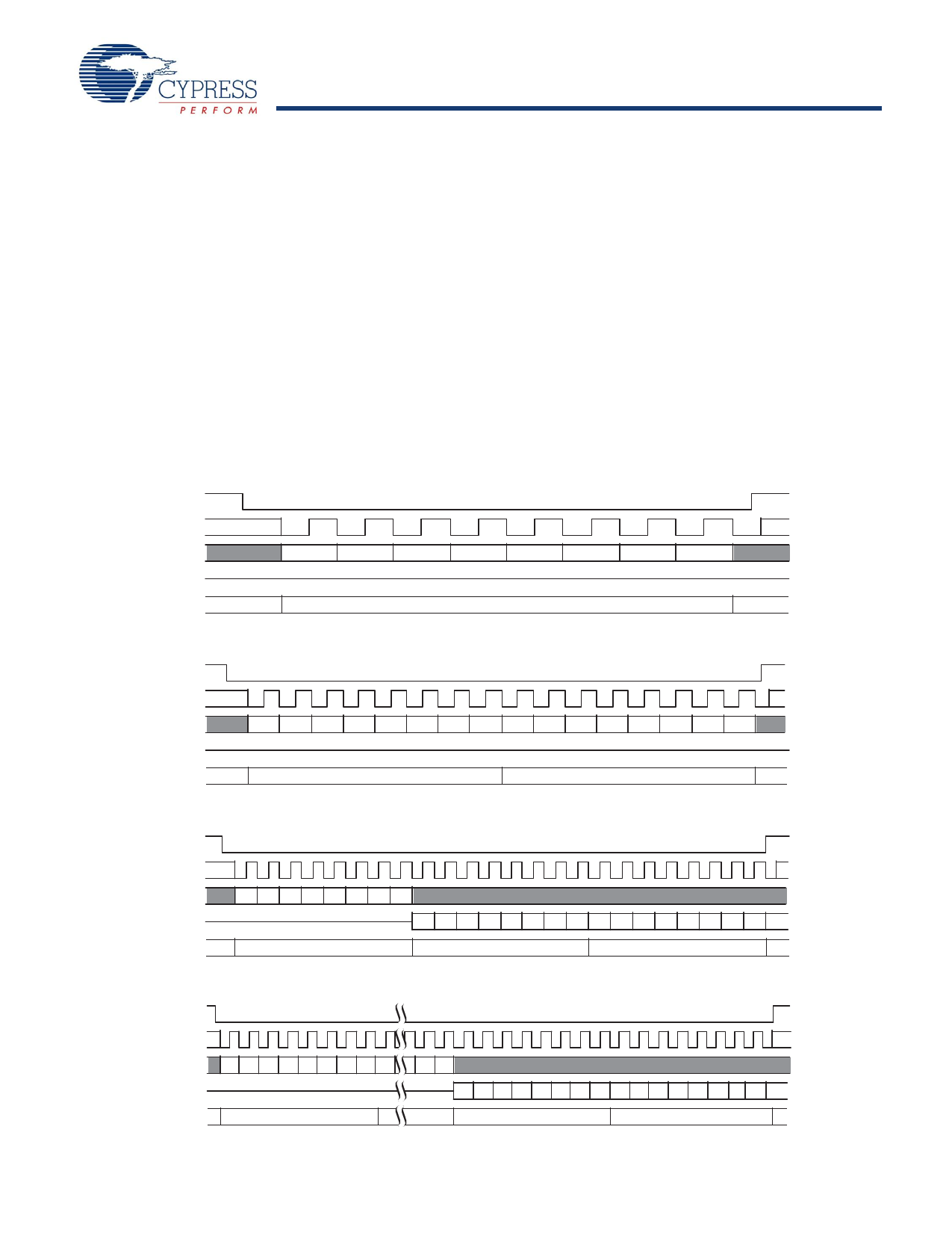
At the end of a command that does not return data, the host drives the CS# input high. The CS# signal must go high after the
eighth bit, of a stand alone instruction or, of the last write data byte that is transferred. That is, the CS# signal must be
driven high when the number of clock cycles after CS# signal was driven low is an exact multiple of eight cycles. If the CS#
signal does not go high exactly at the eight SCK cycle boundary of the instruction or write data, the command is rejected
and not executed.
All instruction, address, and mode bits are shifted into the device with the Most Significant Bits (MSB) first. The data bits are
shifted in and out of the device MSB first. All data is transferred in byte units with the lowest address byte sent first.
Following bytes of data are sent in lowest to highest byte address order i.e. the byte address increments.
All attempts to read the flash memory array during a program, erase, or a write cycle (embedded operations) are ignored. The
embedded operation will continue to execute without any affect. A very limited set of commands are accepted during an
embedded operation. These are discussed in the individual command descriptions.
Depending on the command, the time for execution varies. A command to read status information from an executing
command is available to determine when the command completes execution and whether the command was successful.
3.2.1
Command Sequence Examples
CS#
SCK
SI
SO
Phase
Figure 3.3 Stand Alone Instruction Command
7
6
5
4
3
2
1
0
Instruction
CS#
SCK
SI
SO
Phase
Figure 3.4 Single Bit Wide Input Command
76 543210 765432 10
Instruction
Input Data
CS#
SCK
SI
SO
Phase
Figure 3.5 Single Bit Wide Output Command
76543210
7 6 5 43 2 1 0 7 6 5 4 3 2 1 0
Instruction
Data 1
Data 2
CS#
SCK
SI
SO
Phase
Figure 3.6 Single Bit Wide I/O Command without Latency
7 6 5 4 3 2 1 0 31 1 0
7 65 4 32 1 0 76 5 4 3 210
Instruction
Address
Data 1
Data 2
Document Number: 001-98283 Rev. *I
Page 16 of 144
Share Link: