LH28F008SC View Datasheet(PDF) - Sharp Electronics
Part Name
Description
Manufacturer
LH28F008SC Datasheet PDF : 38 Pages
| |||
8M (1M × 8) Flash Memory
LH28F008SC
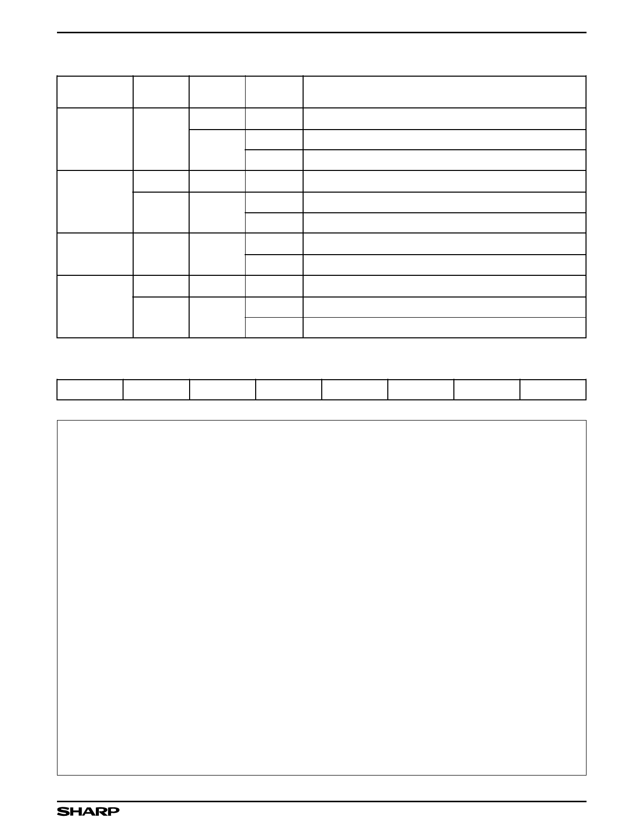
Write Protection Alternatives
OPERATION
MASTER BLOCK
LOCK-BIT LOCK-BIT
RP#
EFFECT
Block Erase or
Byte Write
X
0
Set Block
Lock Bit
1
Set Master
Lock-Bit
X
0
Clear Block
Lock-Bits
1
0
VIH or VHH Block Erase and Byte Write Enabled.
1
VIH
Block is locked. Block Erase and Byte Write Disabled.
VHH
Block Lock-Bit Override. Block Erase and Byte Write Enabled.
X
VIH or VHH Set Block Lock-Bit Enabled.
X
VIH
Master Lock-Bit is Set. Set Block Lock-Bit Disabled.
VHH
Master Lock-Bit Override. Set Block Lock-Bit Enabled.
VIH
Set Master Lock-Bit Disabled.
X
VHH
Set Master Lock-Bit Enabled.
X
VIH or VHH Clear Block Lock-Bits Enable.
X
VIH
Master Lock-Bit is Set. Clear Block Lock-Bits Disabled.
VHH
Master Lock-Bit Override. Clear Block Lock-Bits Enabled.
Status Register Definition
WSMS
7
ESS
6
ECLBS
5
BWSLBS
4
SR.7
= WRITE STATE MACHINE STATUS
1 = Ready
0 = Busy
SR.6
= ERASE SUSPEND STATUS
1 = Block Erase Suspended
0 = Block Erase in Progress/Completed
SR.5
= ERASE AND CLEAR LOCK-BIT STATUS
1 = Error in Block Erasure or Clear Lock-Bits
0 = Successful Block Erase or Clear Lock-Bits
SR.4
= BYTE WRITE AND SET LOCK-BIT STATUS
1 = Error in Byte Write or Set Master/Block Lock Bit
0 = Successful Byte Write or Set Master/Block
0 = Lock-Bit
SR.3
= VPP STATUS (VPPS)
1 = VPP Low Detect, Operation Abort
0 = VPP OK
SR.2
= BYTE WRITE SUSPEND STATUS
1 = Byte Write Suspended
0 = Byte Write in Progress/Completed
SR.1
= DEVICE PROTECT STATUS
1 = Master Lock-Bit, Block Lock-Bit and/or
1 = RP ┬╗ Lock Detected, Operation Abort
0 = Unlock
SR.0 = RESERVED FOR FUTURE ENHANCEMENTS
VPPS
BWSS
DPS
R
3
2
1
0
NOTES:
1. Check RY ┬╗/BY ┬╗ or SR.7 to determine block erase, byte
write, or lock-bit configuration completion. SR.6 - SR.0 are
invalid while SR.7 = '0'.
2. If both SR.5 and SR.4 are '1's after a block erase or lock-
bit configuration attempt, an improper command sequence
was entered.
3. SR.3 does not provide a continuous indication of VPP level.
The WSM interrogates and indicates the VPP level only
after Block Erase, Byte Write, Set Block/Master Lock-Bit,
or Clear Block Lock-Bits command sequences. SR.3 is not
guaranteed to report accurate feedback only when
VPP = VPPH1/2/3.
4. SR.1 does not provide a continuous indication of master
and block lock-bit values. The WSM interrogates the master
lock-bit, block lock-bit, and RP ┬╗ only after Block Erase, Byte
Write, or Lock-Bit configuration command sequences. It
informs the system, depending on the attempted operation,
if the block lock-bit is set, master lock-bit is set, and/or RP ┬╗
is not VHH. Reading the block lock and master lock configu-
ration codes after writing the Read identifier Codes com-
mand indicates master and block lock-bit status.
5. SR.0 is reserved for future use and should be masked out
when polling the status register.
13
Share Link: 