MT48LC1M16A1 View Datasheet(PDF) - Micron Technology
Part Name
Description
Manufacturer
MT48LC1M16A1 Datasheet PDF : 51 Pages
| |||
16Mb: x16
IT SDRAM
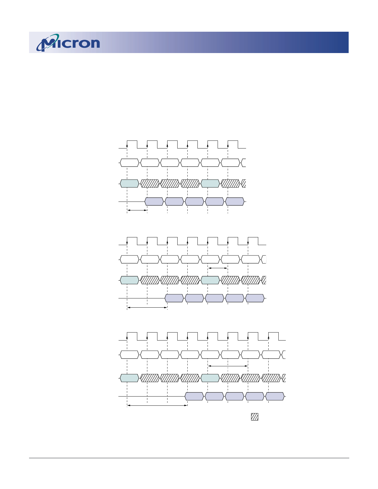
data element is valid, where x equals the CAS latency
minus one. This is shown in Figure 7 for READ latencies
of one, two and three; data element n + 3 is either the
last of a burst of four or the last desired of a longer
burst. The 1 Meg x 16 SDRAM uses a pipelined architec-
ture and therefore does not require the 2n rule associ-
ated with a prefetch architecture. A READ command
can be initiated on any clock cycle following a previous
READ command. Full-speed, random read accesses
within a page can be performed as shown in Figure 8.
16Mb: x16 IT SDRAM
16MSDRAMx16IT.p65 – Rev. 5/99
T0
T1
T2
T3
CLK
T4
T5
COMMAND
READ
NOP
NOP
ADDRESS
BANK,
COL n
NOP
READ
NOP
X = 0 cycles
BANK,
COL b
DQ
DOUT
n
CAS Latency = 1
DOUT
n+1
DOUT
n+2
DOUT
n+3
DOUT
b
T0
T1
T2
T3
T4
T5
T6
CLK
COMMAND
READ
NOP
NOP
NOP
READ
NOP
NOP
ADDRESS
BANK,
COL n
X = 1 cycle
BANK,
COL b
DQ
DOUT
n
DOUT
n+1
DOUT
n+2
DOUT
n+3
DOUT
b
CAS Latency = 2
T0
T1
T2
T3
T4
T5
T6
T7
CLK
COMMAND
READ
NOP
NOP
NOP
READ
NOP
NOP
NOP
ADDRESS
BANK,
COL n
BANK,
COL b
X = 2 cycles
DQ
DOUT
n
DOUT
n+1
DOUT
n+2
CAS Latency = 3
NOTE: Each READ command may be to either bank. DQM is LOW.
DOUT
n+3
DOUT
b
DON’T CARE
Figure 7
Consecutive READ Bursts
14
Micron Technology, Inc., reserves the right to change products or specifications without notice.
©1999, Micron Technology, Inc.
Share Link: 