NT5CB128M8DN View Datasheet(PDF) - Nanya Technology
Part Name
Description
Manufacturer
NT5CB128M8DN Datasheet PDF : 138 Pages
| |||
NT5CB128M8DN/NT5CB64M16DP
NT5CC128M8DN/NT5CC64M16DP
1Gb DDR3 D-die SDRAM
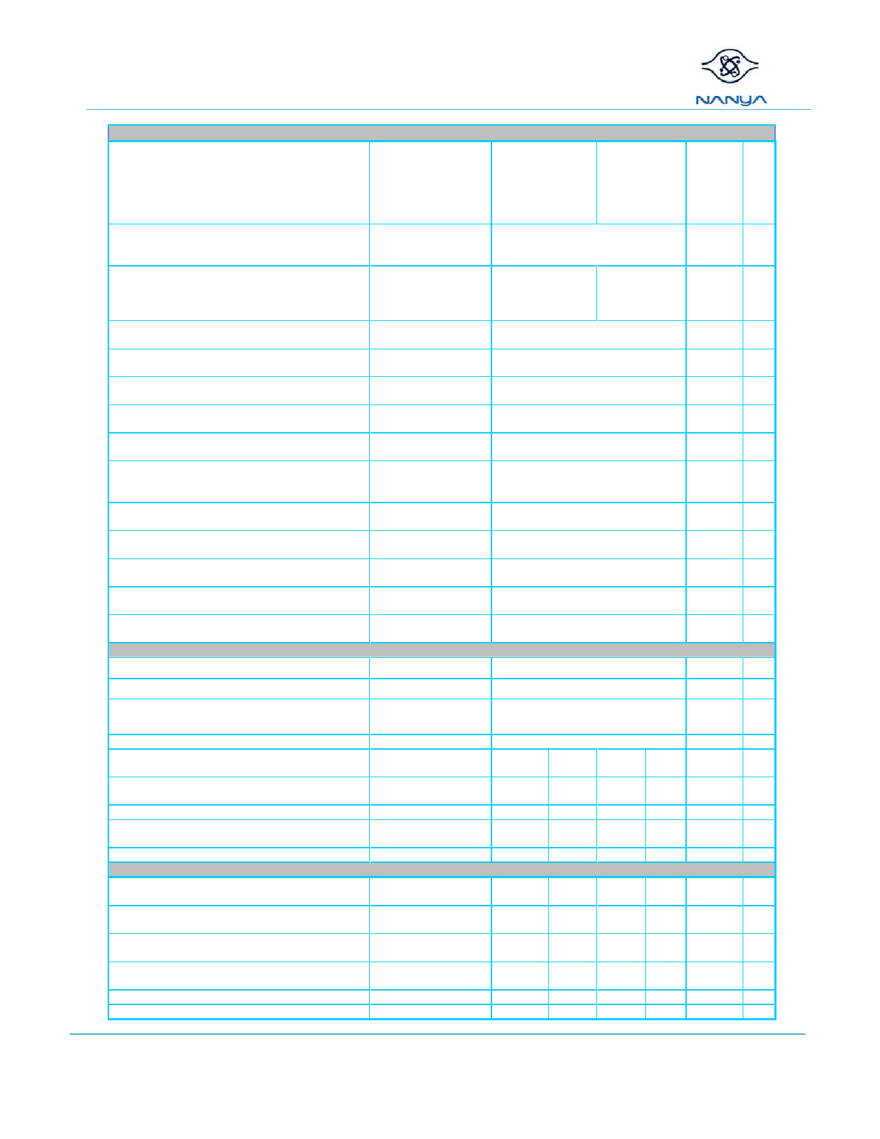
Power Down Timings
Exit Power Down with DLL on to any valid
command;
Exit Precharge Power Down with DLL frozen to tXP
commands
not requiring a locked DLL
Exit Precharge Power Down with DLL frozen to
commands
tXPDLL
requiring a locked DLL
CKE minimum pulse width
tCKE
Command pass disable delay
tCPDED
Power Down Entry to Exit Timing
tPD
Timing of ACT command to Power Down entry tACTPDEN
Timing of PRE or PREA command to Power
Down entry
Timing of RD/RDA command to Power Down
entry
tPRPDEN
tRDPDEN
Timing of WR command to Power Down entry
(BL8OTF, BL8MRS, BC4OTF)
tWRPDEN
Timing of WRA command to Power Down entry
(BL8OTF, BL8MRS, BC4OTF)
tWRAPDEN
Timing of WR command to Power Down entry
(BC4MRS)
tWRPDEN
Timing of WRA command to Power Down entry
(BC4MRS)
tWRAPDEN
Timing of REF command to Power Down entry tREFPDEN
Timing of MRS command to Power Down entry tMRSPDEN
ODT Timings
ODT turn on Latency
ODTLon
ODT turn off Latency
ODTLoff
ODT high time without write command or
with write command and BC4
ODTH4
ODT high time with Write command and BL8
Asynchronous RTT turn-on delay
(Power-Down with DLL frozen)
Asynchronous RTT turn-off delay
(Power-Down with DLL frozen)
RTT turn-on
RTT_Nom and RTT_WR turn-off time
from ODTLoff reference
RTT dynamic change skew
Write Leveling Timings
ODTH8
tAONPD
tAOFPD
tAON
tAOF
tADC
First DQS/DQS# rising edge after
write leveling mode is programmed
tWLMRD
DQS/DQS# delay after write leveling mode is
programmed
tWLDQSEN
Write leveling setup time from rising CK, CK#
crossing to rising DQS, DQS# crossing
tWLS
Write leveling hold time from rising DQS,
crossing to rising CK, CK# crossing
DQS#
tWLH
Write leveling output delay
tWLO
Write leveling output error
tWLOE
tXPmin.:
tXPmin.:
max(3nCK, 7.5ns)
max(3nCK,
6ns)
ʳ
ʳ
tXPmax.: -
tXPmax.: -
tXPDLLmin.: max(10nCK, 24ns)
tXPDLLmax.: -
ʳ
ʳ
tCKEmin.:
tCKEmin.:
max(3nCK ,5.625n max(3nCK ,5.6
s)
25ns)
ʳ
ʳ
tCKEmax.: -
tCKEmax.: -
tCPDEDmin.: 1
tCPDEDmin.: -
nCK
ʳ
tPDmin.: tCKE(min)
tPDmax.: 9*tREFI
ʳ
ʳ
tACTPDENmin.: 1
tACTPDENmax.: -
nCK
ʳ
tPRPDENmin.: 1
tPRPDENmax.: -
nCK
ʳ
tRDPDENmin.: RL+4+1
tRDPDENmax.: -
nCK
ʳ
tWRPDENmin.: WL + 4 + (tWR /
tCK(avg))
nCK
ʳ
tWRPDENmax.: -
tWRAPDENmin.: WL+4+WR+1
tWRAPDENmax.: -
nCK
ʳ
tWRPDENmin.: WL + 2 + (tWR /
tCK(avg))tWRPDENmax.: -
nCK
ʳ
tWRAPDENmin.: WL + 2 +WR + 1
tWRAPDENmax.: -
nCK
ʳ
tREFPDENmin.: 1
tREFPDENmax.: -
nCK
ʳ
tMRSPDENmin.: tMOD(min)
tMRSPDENmax.: -
ʳ
ʳ
WL-2=CWL+AL-2
WL-2=CWL+AL-2
nCK
ʳ
nCK
ODTH4min.: 4;ODTH4max.: -
nCK
ODTH8min.: 6;ODTH8max.: -
nCK
ʳ
2
8.5
2
8.5 ns
ʳ
2
-300
0.3
0.3
8.5
2
8.5 ns
ʳ
300 -250 250 ps
ʳ
0.7
0.3
0.7 tCK(avg) ʳ
0.7
0.3
0.7 tCK(avg) ʳ
40
-
25
-
245
-
245
-
0
9
0
2
40
-
nCK
ʳ
25
-
nCK
ʳ
195 -
ps
ʳ
195 -
ps
ʳ
0
9
ns
ʳ
0
2
ns
ʳ
REV 1.2
May. 2011
CONSUMER DRAM
© NANYA TECHNOLOGY CORP.
All rights reserved
NANYA TECHNOLOGY CORP. reserves the right to change Products and Specifications without notice.
Share Link: 