TC7136 View Datasheet(PDF) - Microchip Technology
Part Name
Description
Manufacturer
TC7136 Datasheet PDF : 22 Pages
| |||
TC7136/TC7136A
1.0 ELECTRICAL
CHARACTERISTICS
Absolute Maximum Ratings*
Supply Voltage (V+ to V-)....................................... 15V
Analog Input Voltage (Either Input) (Note 1)... V+ to V-
Reference Input Voltage (Either Input)............ V+ to V-
Clock Input .................................................TEST to V+
Package Power Dissipation (TA ≤ 70°C) (Note 2):
Plastic DIP ................................................... 1.23W
Plastic Quad Flat Package .......................... 1.00W
PLCC ........................................................... 1.23W
Operating Temperature Range:
C Devices.......................................... 0°C to +70°C
I Devices ........................................ -25°C to +85°C
Storage Temperature Range.............. -65°C to +150°C
*Stresses above those listed under "Absolute Maximum
Ratings" may cause permanent damage to the device. These
are stress ratings only and functional operation of the device
at these or any other conditions above those indicated in the
operation sections of the specifications is not implied.
Exposure to Absolute Maximum Rating conditions for
extended periods may affect device reliability.
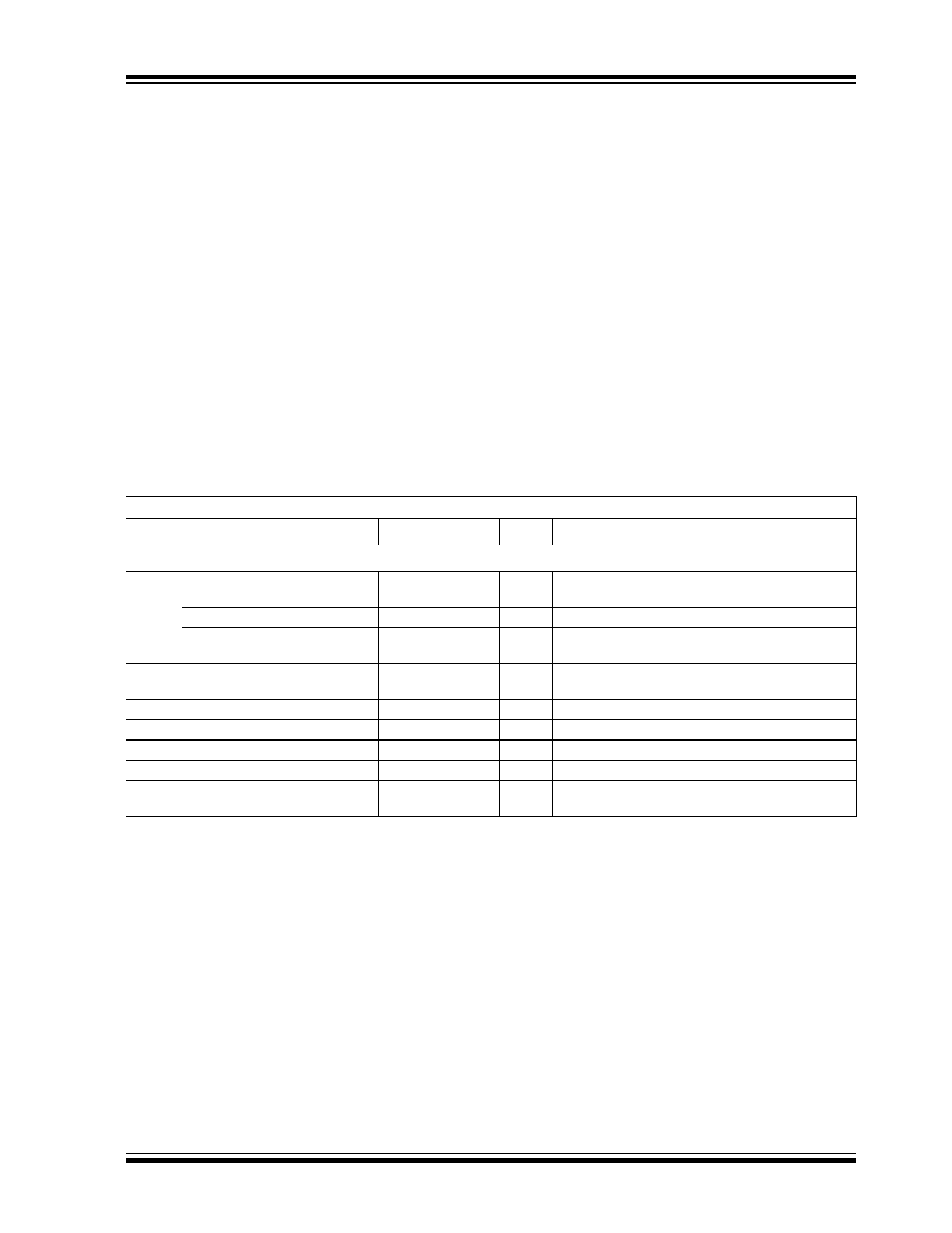
TC7136 AND TC7136A ELECTRICAL SPECIFICATIONS
Electrical Characteristics: VS = 9V, fCLK = 16kHz, and TA = +25°C, unless otherwise noted.
Symbol
Parameter
Min
Typ
Max
Unit
Test Conditions
Input
Zero Input Reading
-000.0
±000.0 +000.0 Digital VIN = 0V, Full Scale = 200mV
Reading
Zero Reading Drift
Ratiometric Reading
—
0.2
1
μV/°C VIN = 0V, 0°C ≤ TA ≤ +70°C
999 999/1000 1000 Digital VIN = VREF, VREF = 100mV
Reading
NL
Non-Linearity Error
—
1
±0.2 Count Full Scale = 20mV or 2V Max.
Deviation from best Straight Line
ER
Rollover Error
-1
eN
Noise
—
IL
Input Leakage Current
—
CMRR Common Mode Rejection Ratio
—
TCSF Scale Factor Temperature
—
Coefficient
-1
±0.2 1 Count VIN- = VIN+ ≈ 200mV
15
—
μVP-P VIN = 0V, Full Scale = 200mV
1
10
pA VIN = 0V
50
—
μV/V VCM = ±1V, VIN = 0V, Full Scale = 200mV
1
5
ppm/°C VIN = 199mV, 0°C ≤ TA ≤ +70°C
Ext. Ref. Temp. Coeff. = 0ppm/°C
Note 1: Input voltages may exceed supply voltages when input current is limited to 100μA.
2: Dissipation rating assumes device is mounted with all leads soldered to PC board.
3: Refer to "Differential Input" discussion.
4: Backplane drive is in phase with segment drive for "OFF" segment and 180° out-of-phase for "ON" segment. Frequency
is 20 times conversion rate. Average DC component is less than 50mV.
5: See "Typical Application".
6: A 48kHz oscillator increases current by 20μA (typical). Common current not included.
© 2005 Microchip Technology Inc.
DS21461C-page 5
Share Link: 