TC7136 View Datasheet(PDF) - Microchip Technology
Part Name
Description
Manufacturer
TC7136 Datasheet PDF : 22 Pages
| |||
TC7136/TC7136A
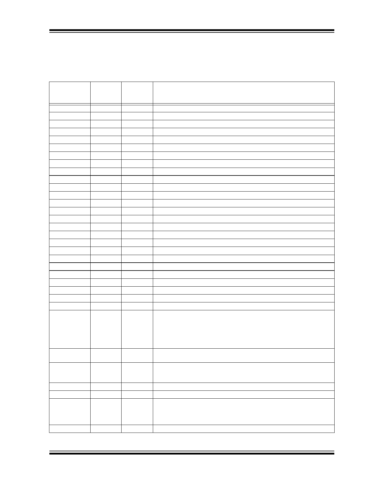
2.0 PIN DESCRIPTIONS
The descriptions of the pins are listed in Table 2-1.
TABLE 2-1:
Pin Number
(40-Pin PDIP)
Normal
1
2
3
4
5
6
7
8
9
10
11
12
13
14
15
16
17
18
19
20
21
22
23
24
25
26
27
28
29
30
31
32
33
PIN DESCRIPTION
(Reverse) Symbol Description
(40)
V+
Positive supply voltage.
(39)
D1
Activates the D section of the units display.
(38)
C1
Activates the C section of the units display.
(37)
B1
Activates the B section of the units display.
(36)
A1
Activates the A section of the units display.
(35)
F1
Activates the F section of the units display.
(34)
G1
Activates the G section of the units display.
(33)
E1
Activates the E section of the units display.
(32)
D2
Activates the D section of the tens display.
(31)
C2
Activates the C section of the tens display.
(30)
B2
Activates the B section of the tens display.
(29)
A2
Activates the A section of the tens display.
(28)
F2
Activates the F section of the tens display.
(27)
E2
Activates the E section of the tens display.
(26)
D3
Activates the D section of the hundreds display.
(25)
B3
Activates the B section of the hundreds display.
(24)
F3
Activates the F section of the hundreds display.
(23)
E3
Activates the E section of the hundreds display.
(22)
AB4
Activates both halves of the 1 in the thousands display.
(21)
POL
Activates the negative polarity display.
(20)
BP
Backplane drive output.
(19)
G3
Activates the G section of the hundreds display.
(18)
A3
Activates the A section of the hundreds display.
(17)
C3
Activates the C section of the hundreds display.
(16)
G2
Activates the G section of the tens display.
(15)
V-
Negative power supply voltage.
(14)
VINT
The integrating capacitor should be selected to give the maximum voltage swing
that ensures component tolerance buildup will not allow the integrator output to sat-
urate. When analog common is used as a reference and the conversion rate is 3
readings per second, a 0.047μF capacitor may be used. The capacitor must have a
low dielectric constant to prevent rollover errors. See Section 6.3, Integrating
Capacitor for additional details.
(13)
VBUFF Integration resistor connection. Use a 180kΩ for a 20mV full scale range and a
1.8MΩ for 2V full scale range.
(12)
CAZ
The size of the auto-zero capacitor influences the system noise. Use a 0.47μF
capacitor for a 200mV full scale and a 0.1μF capacitor for a 2V full scale.
See Section 6.1, Auto-Zero Capacitor for more details.
(11)
VIN-
The low input signal is connected to this pin.
(10)
VIN+
The high input signal is connected to this pin.
(9)
ANALOG This pin is primarily used to set the Analog Common mode voltage for battery
COMMON operation, or in systems where the input signal is referenced to the power supply.
See Section 7.3, Analog Common for more details. It also acts as a reference
voltage source.
(8)
CREF- See Pin 34.
© 2005 Microchip Technology Inc.
DS21461C-page 7
Share Link: 