TC7136 View Datasheet(PDF) - Microchip Technology
Part Name
Description
Manufacturer
TC7136 Datasheet PDF : 22 Pages
| |||
TC7136/TC7136A
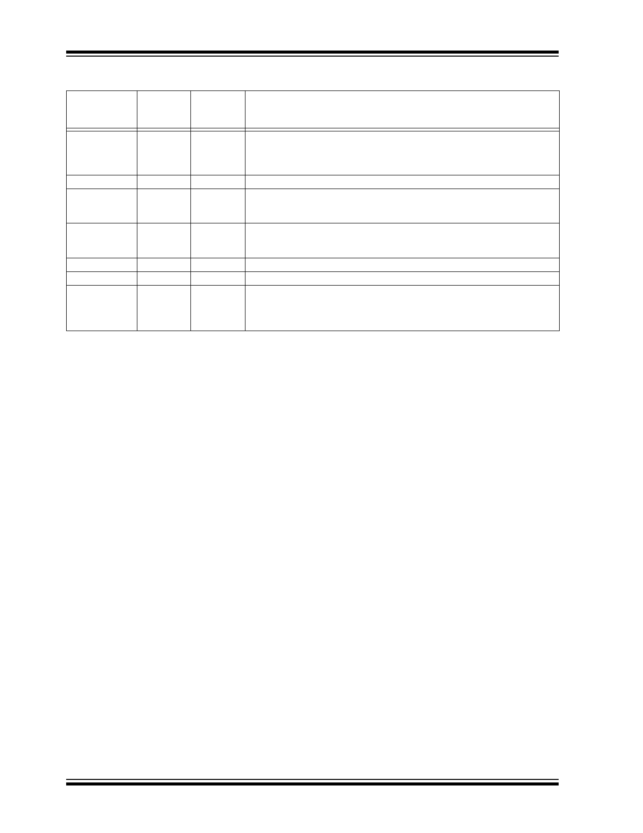
TABLE 2-1:
Pin Number
(40-Pin PDIP)
Normal
34
35
36
37
38
39
PIN DESCRIPTION (CONTINUED)
(Reverse) Symbol Description
(7)
CREF+ A 0.1μF capacitor is used in most applications. If a large Common mode voltage
exists (for example, the VIN- pin is not at analog common) and a 200mV scale is
used, a 1μF capacitor is recommended, which will hold the rollover error to
0.5 count.
(6)
VREF-
See Pin 36.
(5)
VREF+ The analog input required to generate a full scale output (1999 counts). Place
100mV between Pins 35 and 36 for 199.9mV full scale. Place 1V between Pins 35
and 36 for 2V full scale. See Section 6.6, Reference Voltage.
(4)
TEST Lamp test. When pulled HIGH (to V+), all segments will be turned ON and the
display should read -1888. It may also be used as a negative supply for externally
generated decimal points. See Section 7.4, Test for additional information.
(3)
OSC3 See Pin 40.
(2)
OSC2 See Pin 40.
(1)
OSC1 Pins 40, 39 and 38 make up the oscillator section. For a 48kHz clock
(3 readings per second), connect Pin 40 to the junction of a 180kΩ resistor and a
50pF capacitor. The 180kΩ resistor is tied to Pin 39 and the 50pF capacitor is tied
to Pin 38.
DS21461C-page 8
© 2005 Microchip Technology Inc.
Share Link: 