TC7136 View Datasheet(PDF) - Microchip Technology
Part Name
Description
Manufacturer
TC7136 Datasheet PDF : 22 Pages
| |||
3.0 DETAILED DESCRIPTION
(All Pin Designations Refer to 40-Pin PDIP.)
3.1 Dual Slope Conversion Principles
The TC7136/A is a dual slope, integrating analog-to-
digital converter. An understanding of the dual slope
conversion technique will aid in following detailed
TC7136/A operational theory.
The conventional dual slope converter measurement
cycle has two distinct phases (see Figure 3-1).
1. Input signal integration
2. Reference voltage integration (de-integration)
The input signal being converted is integrated for a
fixed time period (tSI), measured by counting clock
pulses. An opposite polarity constant reference voltage
is then integrated until the integrator output voltage
returns to zero. The reference integration time is
directly proportional to the input signal (tRI).
In a simple dual slope converter, a complete conver-
sion requires the integrator output to "ramp up" and
"ramp down."
A simple mathematical equation relates the input
signal, reference voltage, and integration time:
EQUATION 3-1:
∫ ---1-----
RC
tSI
0
VIN(t)dt
=
V----R---t--R---I
RC
Where:
VR = Reference voltage
tSI = Signal integration time (fixed)
tRI = Reference voltage integration time
(variable)
For a constant VIN:
EQUATION 3-2:
VIN
=
VR
t--R-----I
tSI
TC7136/TC7136A
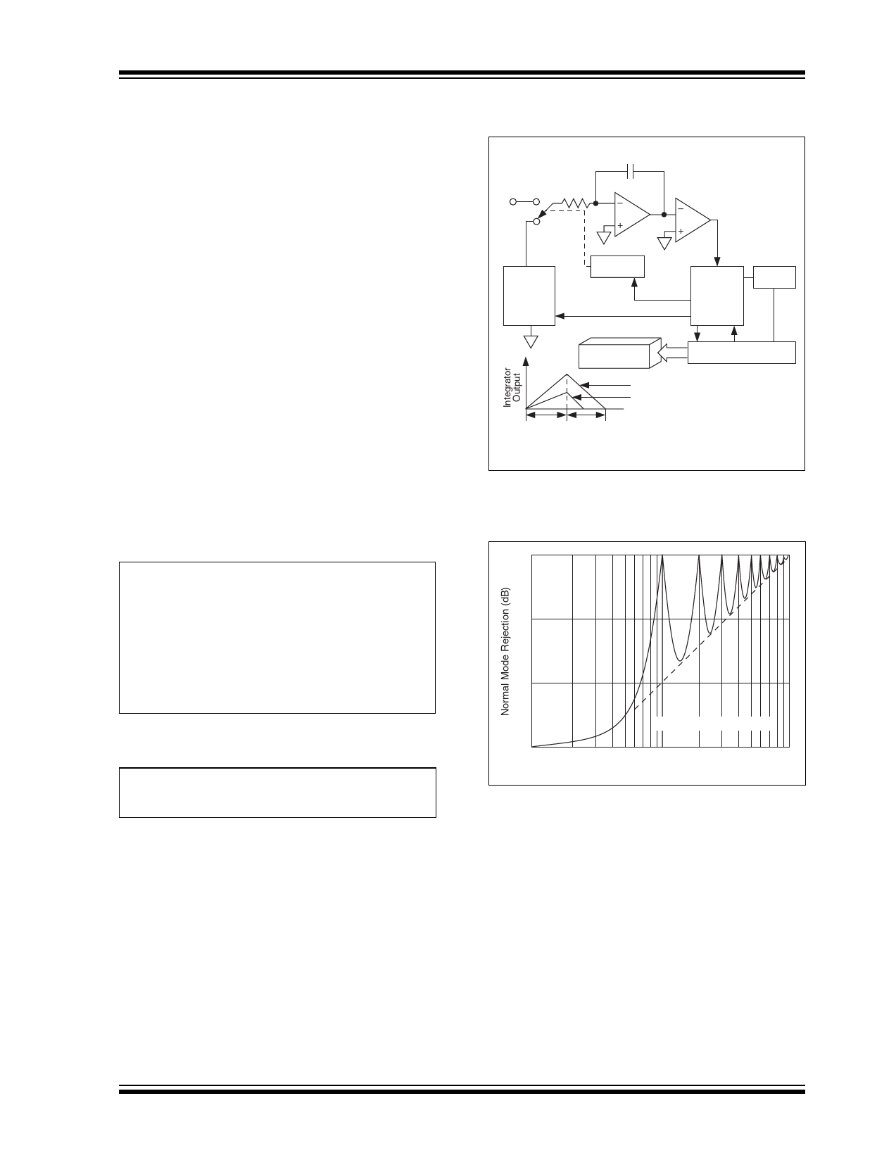
FIGURE 3-1:
Analog Input
Signal
BASIC DUAL SLOPE
CONVERTER
CINT
Integrator
–
+
–Comparator
+
REF
Voltage
Switch
Driver
Phase
Control
Polarity Control
Control
Logic
Clock
Display
VIN ≈ VREF
VIN ≈ 1/2 VREF
Fixed
Signal
Integrate
Time
Variable
Reference
Integrate
Time
Counter
FIGURE 3-2:
30
NORMAL MODE
REJECTION OF DUAL
SLOPE CONVERTER
20
10
0
0.1/t
t = Measured Period
1/t
10/t
Input Frequency
The dual slope converter accuracy is unrelated to the
integrating resistor and capacitor values, as long as
they are stable during a measurement cycle. Noise
immunity is an inherent benefit. Noise spikes are inte-
grated or averaged to zero during integration periods.
Integrating ADCs are immune to the large conversion
errors that plague successive approximation convert-
ers in high noise environments. Interfering signals with
frequency components at multiples of the averaging
period will be attenuated. Integrating ADCs commonly
operate with the signal integration period set to a
multiple of the 50Hz/60Hz power line period.
© 2005 Microchip Technology Inc.
DS21461C-page 9
Share Link: 