S25FL127SABMFI003 View Datasheet(PDF) - Cypress Semiconductor
Part Name
Description
Manufacturer
S25FL127SABMFI003 Datasheet PDF : 142 Pages
| |||
S25FL127S
3. Signal Protocols
3.1 SPI Clock Modes
3.1.1
Single Data Rate (SDR)
The S25FL-S family of devices can be driven by an embedded microcontroller (bus master) in either of the two following clocking
modes.
Mode 0 with Clock Polarity (CPOL) = 0 and, Clock Phase (CPHA) = 0
Mode 3 with CPOL = 1 and, CPHA = 1
For these two modes, input data into the device is always latched in on the rising edge of the SCK signal and the output data is
always available from the falling edge of the SCK clock signal.
The difference between the two modes is the clock polarity when the bus master is in standby mode and not transferring any data.
SCK will stay at logic low state with CPOL = 0, CPHA = 0
SCK will stay at logic high state with CPOL = 1, CPHA = 1
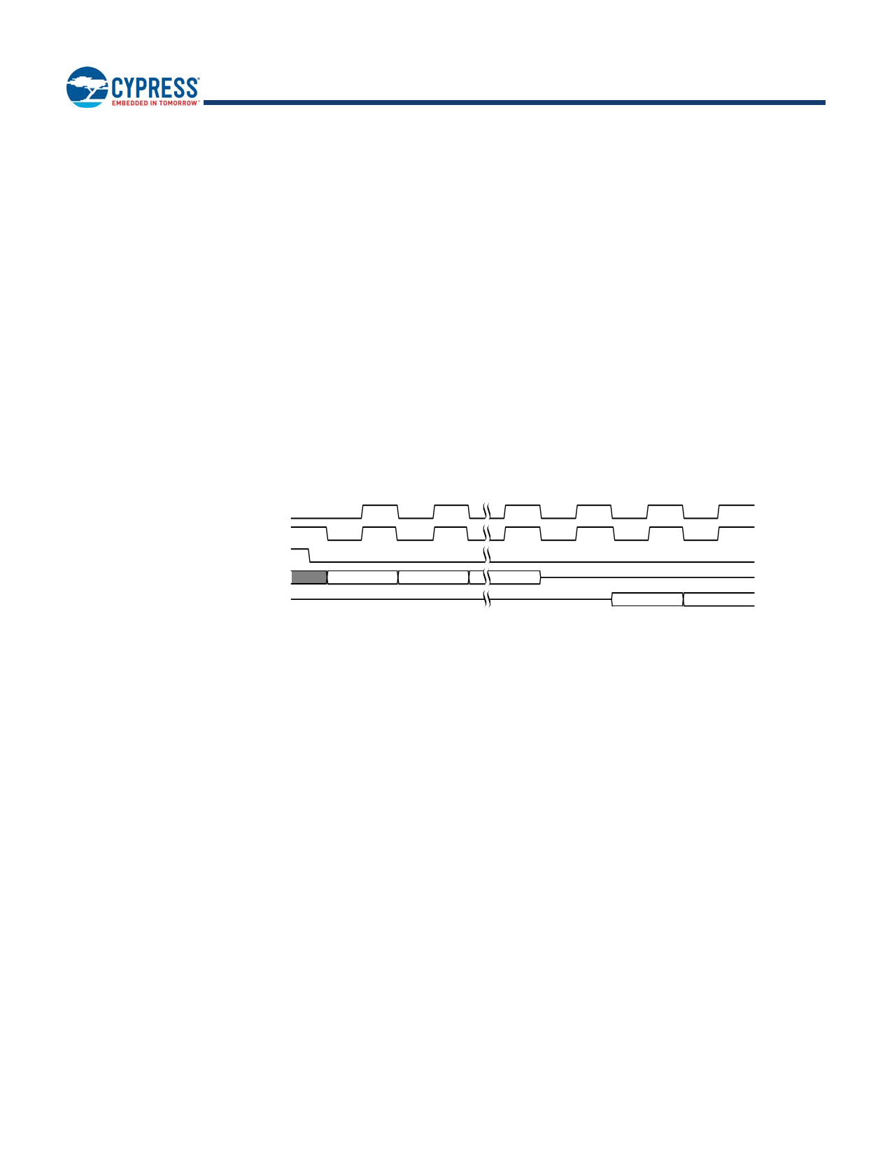
Figure 5. SPI Modes Supported
POL=0_CPHA=0_SCLK
POL=1_CPHA=1_SCLK
CS#
SI
SO
MSB
MSB
Timing diagrams throughout the remainder of the document are generally shown as both mode 0 and 3 by showing SCK as both
high and low at the fall of CS#. In some cases a timing diagram may show only mode 0 with SCK low at the fall of CS#. In such a
case, mode 3 timing simply means clock is high at the fall of CS# so no SCK rising edge set up or hold time to the falling edge of
CS# is needed for mode 3.
SCK cycles are measured (counted) from one falling edge of SCK to the next falling edge of SCK. In mode 0 the beginning of the
first SCK cycle in a command is measured from the falling edge of CS# to the first falling edge of SCK because SCK is already low
at the beginning of a command.
3.2 Command Protocol
All communication between the host system and S25FL-S family of memory devices is in the form of units called commands.
All commands begin with an instruction that selects the type of information transfer or device operation to be performed. Commands
may also have an address, instruction modifier, latency period, data transfer to the memory, or data transfer from the memory. All
instruction, address, and data information is transferred serially between the host system and memory device.
All instructions are transferred from host to memory as a single bit serial sequence on the SI signal.
Single bit wide commands may provide an address or data sent only on the SI signal. Data may be sent back to the host serially on
the SO signal.
Dual or Quad Output commands provide an address sent to the memory only on the SI signal. Data will be returned to the host as a
sequence of bit pairs on IO0 and IO1 or four bit (nibble) groups on IO0, IO1, IO2, and IO3.
Dual or Quad Input/Output (I/O) commands provide an address sent from the host as bit pairs on IO0 and IO1 or, four bit (nibble)
groups on IO0, IO1, IO2, and IO3. Data is returned to the host similarly as bit pairs on IO0 and IO1 or, four bit (nibble) groups on IO0,
IO1, IO2, and IO3.
Document Number: 001-98282 Rev. *I
Page 15 of 142
Share Link: 