S25FL127SABMFI003 View Datasheet(PDF) - Cypress Semiconductor
Part Name
Description
Manufacturer
S25FL127SABMFI003 Datasheet PDF : 142 Pages
| |||
S25FL127S
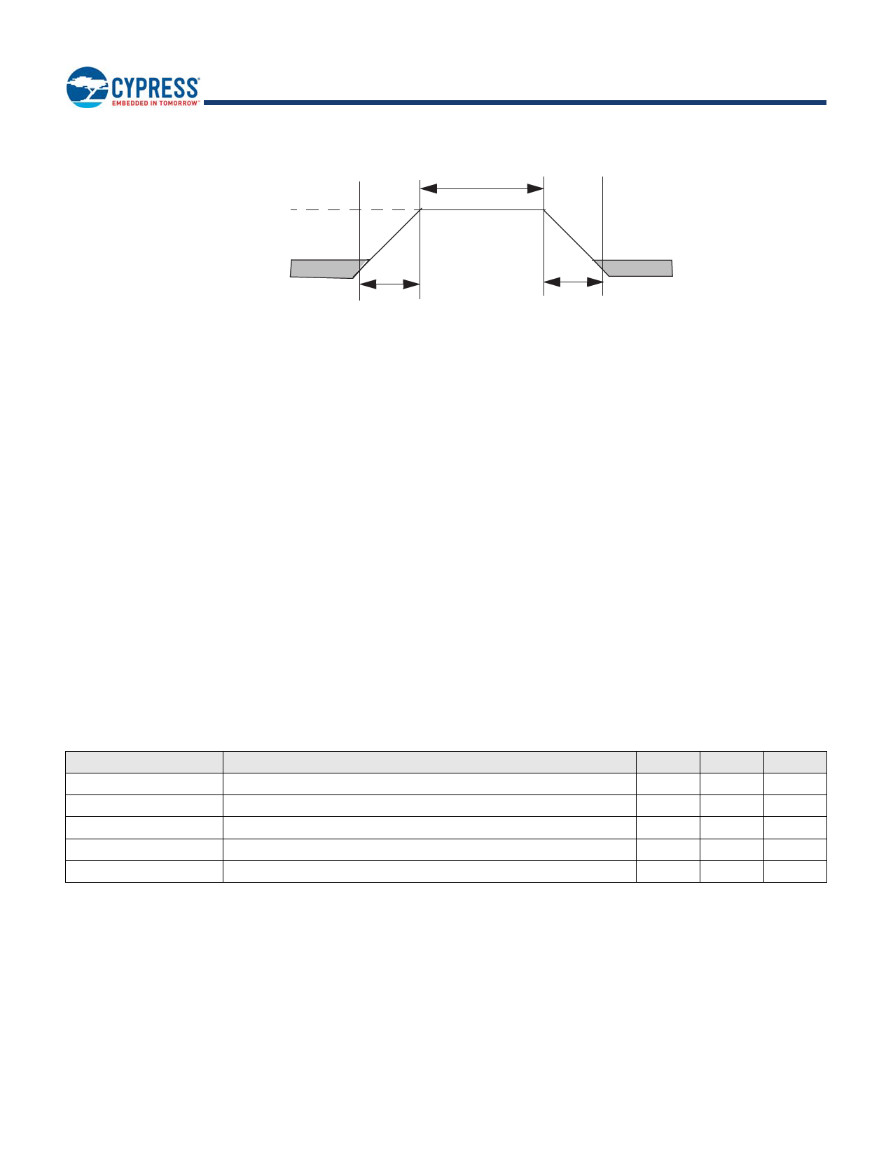
Figure 16. Maximum Positive Overshoot Waveform
20 ns
VCC+ 2.0V
VIH
20 ns
20 ns
4.3 Power-Up and Power-Down
The device must not be selected at power-up or power-down (that is, CS# must follow the voltage applied on VCC) until VCC reaches
the correct value as follows:
VCC (min) at power-up, and then for a further delay of tPU
VSS at power-down
A simple pull-up resistor (generally of the order of 100 kΩ) on Chip Select (CS#) can usually be used to insure safe and proper
power-up and power-down.
The device ignores all instructions until a time delay of tPU has elapsed after the moment that VCC rises above the minimum VCC
threshold. See Figure 17, Power-up on page 27. However, correct operation of the device is not guaranteed if VCC returns below
VCC (min) during tPU. No command should be sent to the device until the end of tPU.
The device draws IPOR during tPU. After power-up (tPU), the device is in Standby mode, draws CMOS standby current (ISB), and the
WEL bit is reset.
During power-down or voltage drops below VCC (cut-off), the voltage must drop below VCC (low) for a period of tPD for the part to
initialize correctly on power-up. See Figure 18, Power-down and Voltage Drop on page 27. If during a voltage drop the VCC stays
above VCC (cut-off) the part will stay initialized and will work correctly when VCC is again above VCC (min). In the event Power-On
Reset (POR) did not complete correctly after power up, the assertion of the RESET# signal or receiving a software reset command
(RESET) will restart the POR process.
Normal precautions must be taken for supply rail decoupling to stabilize the VCC supply at the device. Each device in a system
should have the VCC rail decoupled by a suitable capacitor close to the package supply connection (this capacitor is generally of the
order of 0.1 µf).
Table 7. Power-up/Power-down Voltage and Timing
Symbol
VCC (min)
VCC (cut-off)
VCC (low)
tPU
tPD
Parameter
VCC (minimum operation voltage)
VCC (Cut 0ff where re-initialization is needed)
VCC (low voltage for initialization to occur)
VCC (min) to Read operation
VCC (low) time
Min
Max
Unit
2.7
V
2.4
V
1.0
V
300
µs
1.0
µs
Document Number: 001-98282 Rev. *I
Page 26 of 142
Share Link: 