S25FL127SABMFI003 View Datasheet(PDF) - Cypress Semiconductor
Part Name
Description
Manufacturer
S25FL127SABMFI003 Datasheet PDF : 142 Pages
| |||
S25FL127S
5. Timing Specifications
5.1
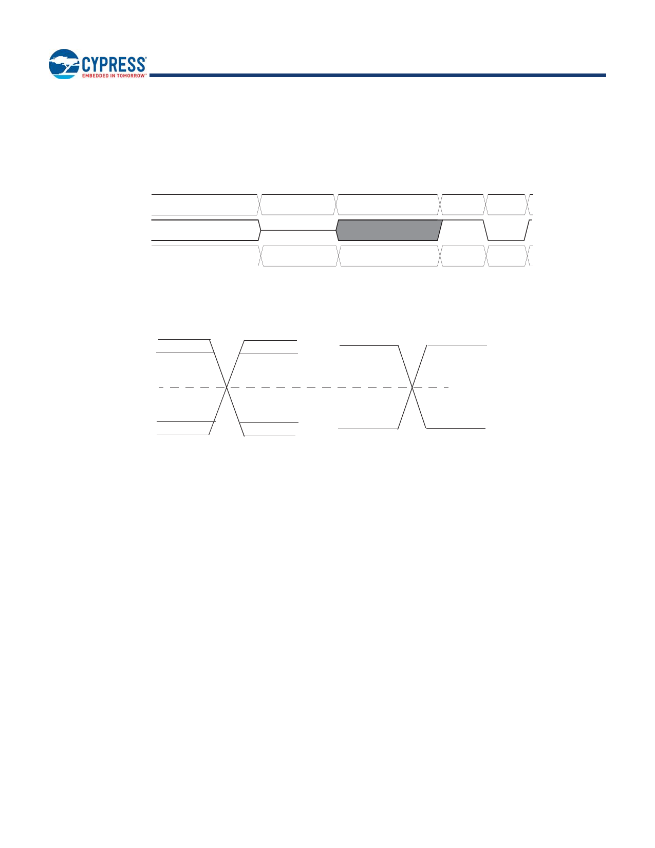
Key to Switching Waveforms
Figure 19. Waveform Element Meanings
Input Valid at logic high or low High Impedance Any change permitted Logic high Logic low
Symbol
Output Valid at logic high or low High Impedance Changing, state unknown Logic high Logic low
Input Levels
VIO + 0.4V
0.7 x VCC
0.5 x VCC
0.2 x VCC
- 0.5V
Figure 20. Input, Output, and Timing Reference Levels
Timing Reference Level
Output Levels
0.85 x VCC
0.15 x VCC
Document Number: 001-98282 Rev. *I
Page 29 of 142
Share Link: 