S25FL127SABMFI003 View Datasheet(PDF) - Cypress Semiconductor
Part Name
Description
Manufacturer
S25FL127SABMFI003 Datasheet PDF : 142 Pages
| |||
S25FL127S
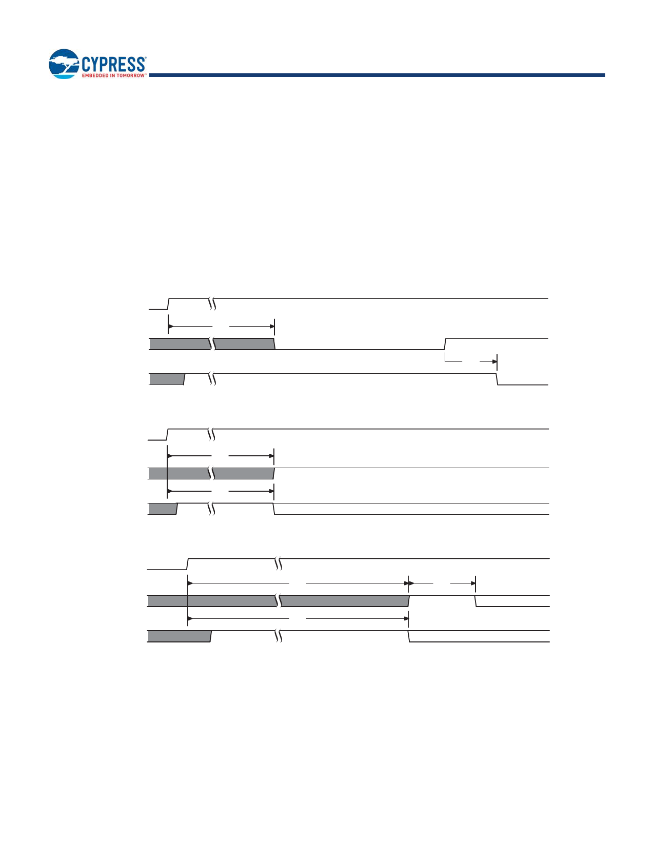
5.3 Reset
5.3.1
Power-On (Cold) Reset
The device executes a Power-On Reset (POR) process until a time delay of tPU has elapsed after the moment that VCC rises above
the minimum VCC threshold. See Figure 17 on page 27, Table 7 on page 26, and Figure 22 on page 31. The device must not be
selected (CS# to go high with VCC) during power-up (tPU), i.e. no commands may be sent to the device until the end of tPU.
The IO3 / RESET# signal functions as the RESET# input when CS# is high for more than tRP time or when Quad Mode is not
enabled CR1V[1]=0.
RESET# is ignored during POR. If RESET# is low during POR and remains low through and beyond the end of tPU, CS# must
remain high until tRH after RESET# returns high. RESET# must return high for greater than tRS before returning low to initiate a
hardware reset.
VCC
RESET#
CS#
Figure 22. Reset Low at the End of POR
tPU
If RESET# is low at tPU end
tRH
CS# must be high at tPU end
VCC
RESET#
CS#
Figure 23. Reset High at the End of POR
tPU
If RESET# is high at tPU end
tPU
CS# may stay high or go low at tPU end
VCC
RESET#
CS#
Figure 24. POR followed by Hardware Reset
tPU
tRS
tPU
Document Number: 001-98282 Rev. *I
Page 31 of 142
Share Link: 