HMP8154 View Datasheet(PDF) - Renesas Electronics
Part Name
Description
Manufacturer
HMP8154 Datasheet PDF : 34 Pages
| |||
HMP8154, HMP8156A
CLK2
P8-P15 Cb 2 Y 2
Cr 2
Y3
Cb 4
Y4
"FF"
"00"
"00"
"XY"
"10"
"80"
"10"
OL0-OL2,
M1, M0
BLANK
(OUTPUT)
PIXEL 0
PIXEL 1
PIXEL N-2
PIXEL N-1
PIXEL N
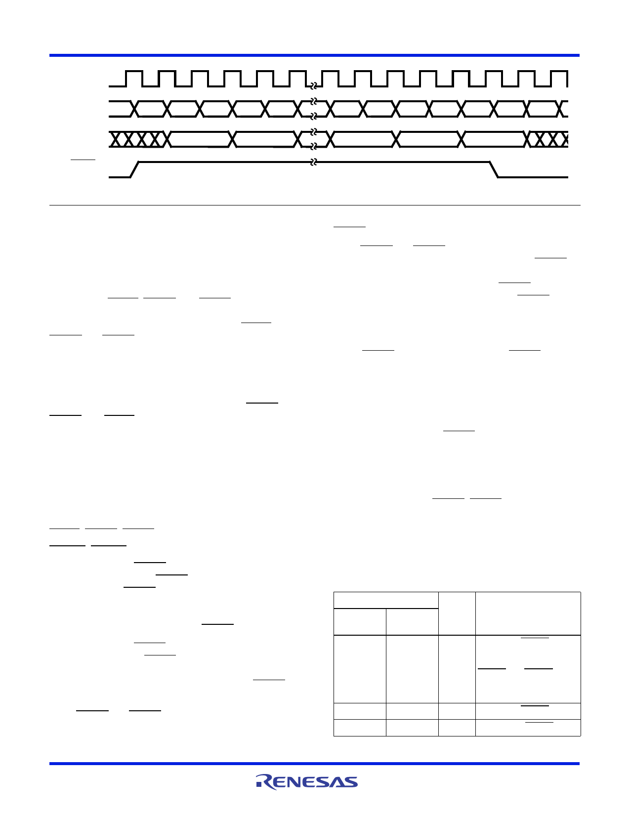
FIGURE 12. PIXEL AND OVERLAY INPUT TIMING - BT.656
8-Bit BT.656 Format
When BT.656 format is selected, data is latched on each
rising edge of CLK2. Overlay data is latched when the Y
input data is latched. However, the overlay data must arrive
three pixels after its corresponding Y data. The pixel and
overlay input timing is shown in Figure 12.
As inputs, the BLANK, HSYNC, and VSYNC pins are
ignored since all timing is derived from the EAV and SAV
sequences within the data stream. As outputs, BLANK,
HSYNC and VSYNC are output following the rising edge of
CLK2. If the CLK pin is configured as an input, it is ignored. If
configured as an output, it is one-half the CLK2 frequency.
Square pixel operation, overlay processing with internal
mixing, flicker filtering, and SIF mode 2X upsampling are not
supported for the BT.656 input format. Also, the HSYNC,
VSYNC, and BLANK signals must be configured as outputs.
Video Timing Control
Regardless of the input mode, the output video timing of the
HMP8154/HMP8156A is at 50 or 59.94 fields per second
(interlaced). For normal and 2X upscaling modes, the pixel
input timing is at 50 or 59.94 fields per second; with the
flicker filter enabled, the input timing rate is twice as fast.
The output video and pixel input timing is controlled by the
BLANK, HSYNC, VSYNC, FIELD, and CLK2 pins.
HSYNC, VSYNC, and Field Timing
The leading edge of HSYNC indicates the beginning of a
horizontal sync interval. If HSYNC is an output, it is asserted
for about 4.7s. If HSYNC is an input, it must be active for at
least two CLK2 periods. The width of the horizontal
composite sync tip is determined from the video standard
and does not depend on the width of HSYNC.
The leading edge of VSYNC indicates the beginning of a
vertical sync interval. If VSYNC is an output, it is asserted for
3 scan lines in (M, NSM) NTSC and (M, N) PAL modes or
2.5 scan lines in (B, D, G, H, I, CN) PAL modes. If VSYNC is
an input, it must be asserted for at least two CLK2 periods.
When HSYNC and VSYNC are configured as outputs, their
leading edges will occur simultaneously at the start of an odd
field. At the start of an even field, the leading edge of
VSYNC occurs in the middle of the line.
When HSYNC and VSYNC are configured as inputs, the
HMP8154/HMP8156A provides a programmable HSYNC
window for determining FIELD. The window is specified with
respect to the leading or trailing edge of VSYNC. The edge
is selected in the field control register. When HSYNC is
found inside the window, then the encoder sets FIELD to the
value specified in the field control register.
The HMP8154/HMP8156A provides programmable timing
for the VSYNC input. At the active edge of VSYNC, the
encoder resets its vertical half-line counter to the value
specified by the field control register. This allows the input
and output syncs to be offset, although the data must still be
aligned.
The FIELD signal is always an output and changes state
near each leading edge of VSYNC. The delay between the
syncs and FIELD depends on the encoder’s operating mode
as summarized in Table 6. In modes in which the encoder
uses CLK to gate its inputs and outputs, the FIELD signal
may be delayed 0-12 additional CLK2 periods.
Figure 13 illustrates the HSYNC, VSYNC, and FIELD
general timing for (M, NSM) NTSC and (M, N) PAL. Figure
14 illustrates the general timing for (B, D, G, H, I, CN) PAL. In
the figures, all the signals are shown active low (their reset
state), and FIELD is low during odd fields.
TABLE 6. FIELD OUTPUT TIMING
OPERATING MODE
SYNC I/O BLANK I/O CLK2
DIRECTION DIRECTION DELAY
COMMENTS
Input
Input
148 FIELD lags VSYNC
switching from odd to even.
FIELD lags the earlier of
VSYNC and HSYNC when
syncs are aligned when
switching from even to odd.
Input
Output
138 FIELD lags VSYNC.
Output
Don’t Care
32 FIELD leads VSYNC.
FN4343 Rev.5.00
August 20, 2009
Page 11 of 34
Share Link: 