S25FL127SABMFI003 View Datasheet(PDF) - Cypress Semiconductor
Part Name
Description
Manufacturer
S25FL127SABMFI003 Datasheet PDF : 142 Pages
| |||
S25FL127S
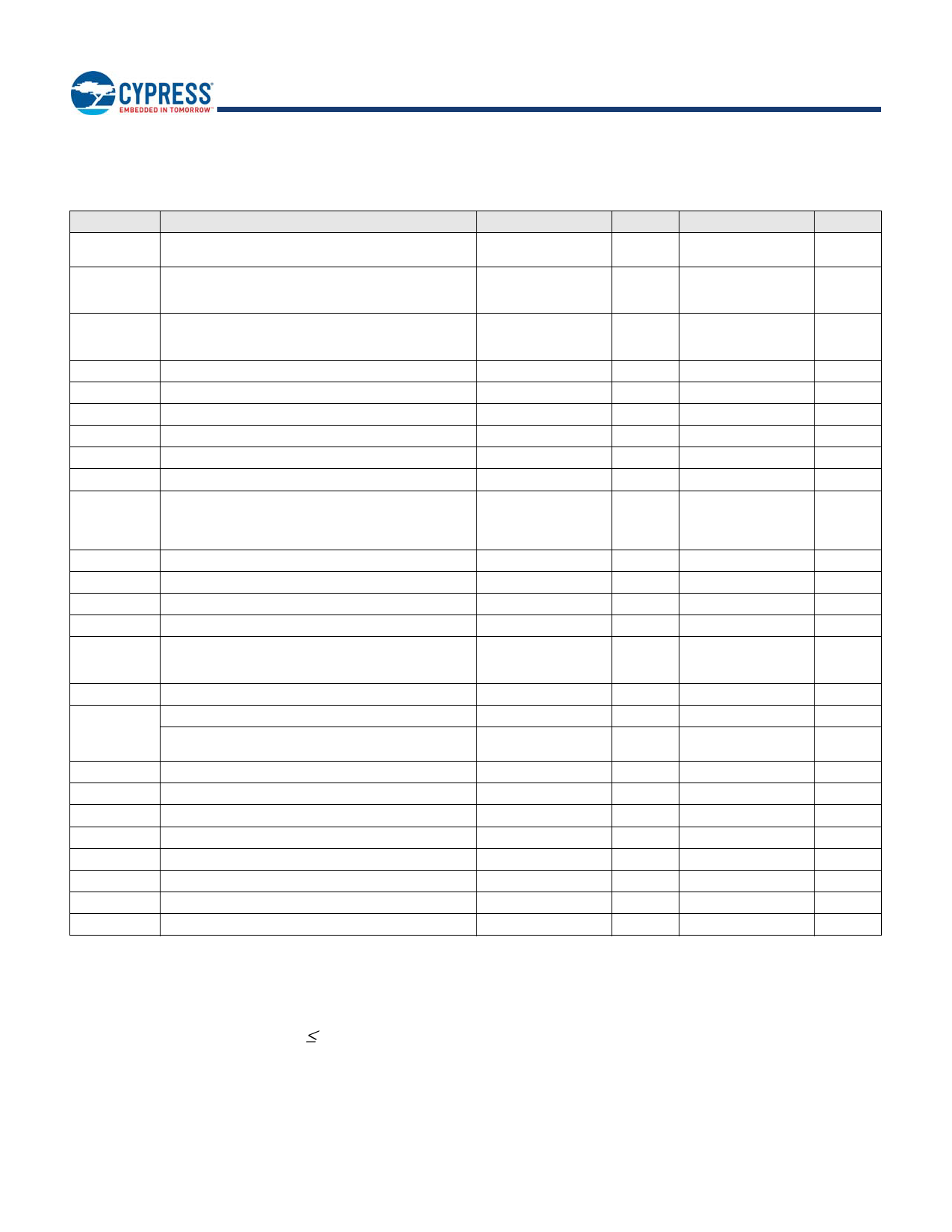
5.4 AC Characteristics
Table 13. AC Characteristics
Symbol
Parameter
Min
Typ
FSCK, R
SCK Clock Frequency for READ and 4READ
instructions
DC
SCK Clock Frequency for single commands as shown in
FSCK, C
Table 36, S25FL127S Command Set (sorted by
function) on page 68 (4)
DC
SCK Clock Frequency for the following dual and quad
FSCK, C
commands: DOR, 4DOR, QOR, 4QOR, DIOR, 4DIOR,
QIOR, 4QIOR
DC
FSCK, QPP
PSCK
tWH, tCH
tWL, tCL
tCRT, tCLCH
tCFT, tCHCL
tCS
SCK Clock Frequency for the QPP, 4QPP commands
SCK Clock Period
Clock High Time (5)
Clock Low Time (5)
Clock Rise Time (slew rate)
Clock Fall Time (slew rate)
CS# High Time (Read Instructions) CS# High Time
(Read Instructions when Reset feature and Quad mode
are both enabled) CS# High Time (Program/Erase
Instructions)
DC
1/ FSCK
50% PSCK -5%
50% PSCK -5%
0.1
0.1
10
20 (7)
50
tCSS
CS# Active Setup Time (relative to SCK)
3
tCSH
CS# Active Hold Time (relative to SCK)
3
tSU
Data in Setup Time
1.5
tHD
Data in Hold Time
2
tV
Clock Low to Output Valid
1
tHO
tDIS
tWPS
tWPH
tHLCH
tCHHH
tHHCH
tCHHL
tHZ
tLZ
Output Hold Time
Output Disable Time (6)
Output Disable Time (when Reset feature and Quad
mode are both enabled)
WP# Setup Time
WP# Hold Time
HOLD# Active Setup Time (relative to SCK)
HOLD# Active Hold Time (relative to SCK)
HOLD# Non Active Setup Time (relative to SCK)
HOLD# Non Active Hold Time (relative to SCK)
HOLD# enable to Output Invalid
HOLD# enable to Output Valid
2
20 (1)
100 (1)
3
3
3
3
Notes:
1. Only applicable as a constraint for WRR instruction when SRWD is set to a 1.
2. Full VCC range (2.7 - 3.6V) and CL = 30 pF.
3. Regulated VCC range (3.0 - 3.6V) and CL = 30 pF.
≤ 4. Regulated VCC range (3.0 - 3.6V) and CL = 15 pF.
5. ±10% duty cycle is supported for frequencies 50 MHz.
6. Output High -Z is defined as the point where data is no longer driven.
7. tCS and tDIS require additional time when the Reset feature and Quad mode are enabled (CR2V[5]=1 and CR1V[1]=1).
Max
50
108
108
80
∞
50% PSCK +5%
50% PSCK +5%
8.0 (2)
7.65 (3)
6.5 (4)
8
20 (7)
8
8
Unit
MHz
MHz
MHz
MHz
ns
ns
V/ns
V/ns
ns
ns
ns
ns
ns
ns
ns
ns
ns
ns
ns
ns
ns
ns
ns
ns
ns
Document Number: 001-98282 Rev. *I
Page 34 of 142
Share Link: 