DSP16410C View Datasheet(PDF) - Agere -> LSI Corporation
Part Name
Description
Manufacturer
DSP16410C Datasheet PDF : 373 Pages
| |||
Data Addendum
May 2001
DSP16410C Digital Signal Processor
5 Ball Grid Array Information (continued)
5.2 256-Ball EBGA Package (continued)
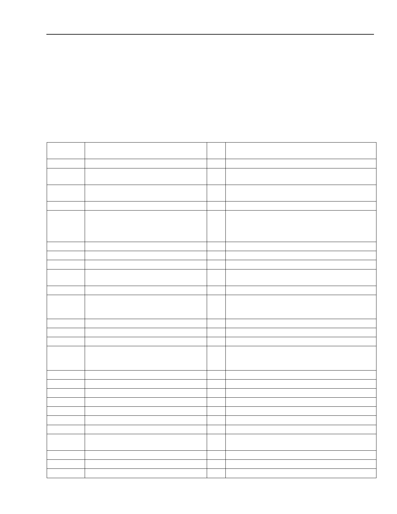
Table 3 describes the EBGA ball assignments sorted by symbol for the 256-ball package. For each signal or
power/ground connection, this table lists the EBGA coordinate, the symbol name, the type (I = input, O = output,
I/O = input/output, O/Z = 3-state output, P = power, G = ground), and description. Inputs and bidirectional pins do
not maintain full CMOS levels when not driven. They must be pulled to VDD2 or VSS through the appropriate pull
up/down resistor (refer to Section 7.1). An unused external SEMI data bus (ED[31:0]) can be statically configured
as outputs by asserting the EYMODE pin. At full CMOS levels, no significant dc current is drawn.
Table 3. 256-Ball EBGA Ball Assignments Sorted Alphabetically by Symbol
Symbol
PBGA
Coordinate
Type
Description
CKI
J19
I External Clock Input.
EA[18:0] B3, C1, C2, C4, D1, D2, D5, E2, E3, E4, F3, O External Address Bus, Bits 18—0.
F4, G2, G3, H2, H3, H4, J3, J4
EACKN
C6
O External Device Acknowledge for External Memory
Interface (negative assertion).
ECKO
M1
O Programmable Clock Output.
ED[31:0]
A8, A9, A10, A14, A17, A18, B6, B8, B9,
B10, B11, B12, B13, B14, B16, B17, C8,
C11, C12, C13, C14, C15, C16, C19, C20,
D7, D10, D15, D16, D18, D19, E17
I/O External Memory Data Bus, Bits 31—0.
EION
A3
O Enable for External I/O (negative assertion).
ERAMN
B4
O External RAM Enable (negative assertion).
ERDY
F17
I External Memory Device Ready.
EREQN
D20
I External Device Request for EMI Interface (negative
assertion).
EROMN
D6
O Enable for External ROM (negative assertion).
ERTYPE
G17
I EROM Type Control:
If 0, asynchronous SRAM mode.
If 1, synchronous SRAM mode.
ERWN0
B5
O Read/Write, Bit 0 (negative assertion).
ERWN1
A4
O Read/Write, Bit 1 (negative assertion).
ESEG[3:0]
K2, L1, L2, L4
O External Segment Address, Bits 3—0.
ESIZE
E19
I External Memory Bus Size Control:
If 0, 16-bit external interface.
If 1, 32-bit external interface.
EXM
F18
I External Boot-up Control for CORE0.
EYMODE
U16
I External Data Bus Mode Configuration Pin.
INT[3:0]
K18, L18, L19, M18
I External Interrupt Requests 3—0.
IO0BIT[6:0] R17, R18, T18, T19, U19, U20, W18
I/O BIO0 Status/Control, Bits 6—0.
IO1BIT[6:0]
T4, U3, U5, V2, V5, W4, Y3
I/O BIO1 Status/Control, Bits 6—0.
PADD[3:0]
U6, V6, W5, Y4
I PIU Address, Bits 3—0.
PCSN
V7
I PIU Chip Select (negative assertion).
PD[15:0] U11, U14, U15, V13, V15, W11, W12, W13, I/O PIU Data Bus, Bits 15—0.
W15, W16, W17, Y11, Y12, Y13, Y17, Y18
PIBF
W10
O PIU Input Buffer Full Flag.
PIDS
Y7
I PIU Input Data Strobe.
PINT
W9
O PIU Interrupt Request To Host.
Agere Systems Inc.
11
Share Link: 