RM7000-250T View Datasheet(PDF) - PMC-Sierra
Part Name
Description
Manufacturer
RM7000-250T Datasheet PDF : 54 Pages
| |||
RM7000™ Microprocessor with On-Chip Secondary Cache Datasheet
Released
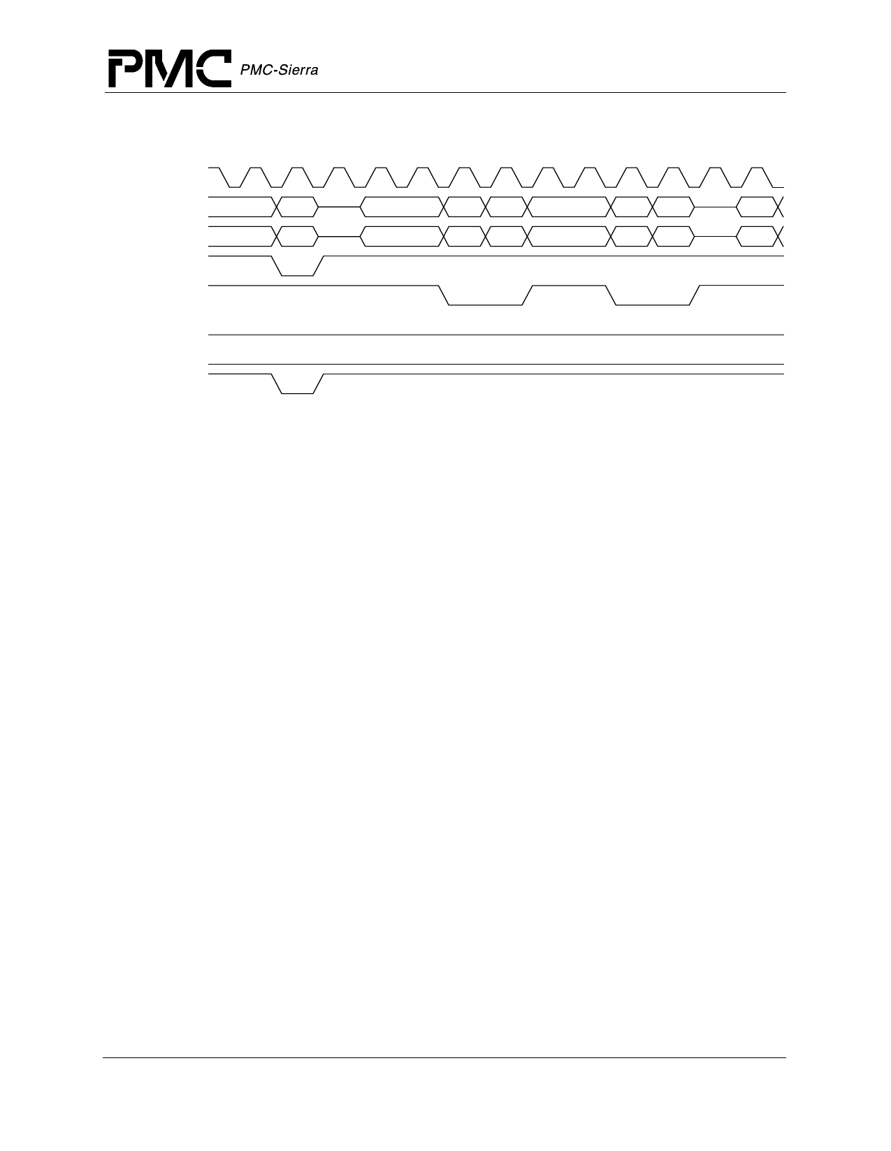
Figure 9 Processor Block Read
SysClock
SysAD
SysCmd
ValidOut*
Addr
Read
ValidIn*
RdRdy*
WrRdy*
Release*
Data0 Data1
NData NData
Data2 Data3
NData NEOD
The read latency is four cycles (ValidOut* to ValidIn*), and the response data pattern is
DDxxDD. Figure 10 shows a processor block write where the processor was programmed with
write-back data rate boot code 2, or DDxxDDxx.
Finally, Figure 11 shows a typical sequence resulting in two outstanding reads both with initial
tertiary cache accesses, as explained in the following sequence.
1. The processor issues a read which misses in the tertiary cache.
2. The external agent takes control of the bus in preparation for returning data to the processor.
3. The processor encounters another internal cache miss and therefore asserts PRqst* in order to
regain control of the bus.
4. The external agent pulses PAck*, returning control of the bus to the processor.
5. The processor issues a read for the second miss.
6. The second cycle also misses in the tertiary.
7. The RspSwap* pin is asserted to denote the out of order response. Not shown in the figure is
the completion of the data transfer for the second miss, or any of the data transfer for the first
miss.
8. The external agent retakes control of the bus and begins returning data (out of order) for the
second miss to the processor.
Proprietary and Confidential to PMC-Sierra, Inc and for its Customer’s Internal Use
30
Document ID: PMC-2002175, Issue 1
Share Link: 