ADM9240 View Datasheet(PDF) - ON Semiconductor
Part Name
Description
Manufacturer
ADM9240 Datasheet PDF : 22 Pages
| |||
ADM9240
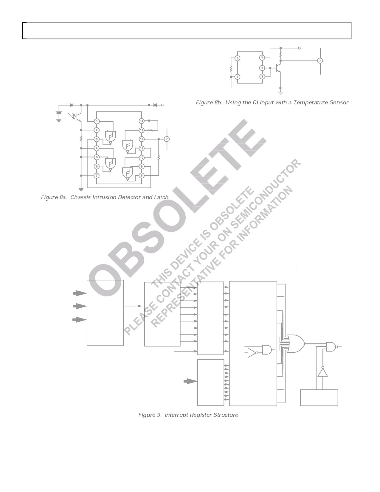
The chassis intrusion circuit should be designed so that it can be
reset by pulling its output low. A suitable chassis intrusion cir-
cuit using a phototransistor is shown in Figure 8. Light falling
on the phototransistor when the PC cover is removed will cause
it to turn on and pull up the input of N1, thus setting the latch
N3/N4. After the cover is replaced, a low reset on the CI output
will pull down the input of N4, resetting the latch.
RSET
AD22105
TEMP.
SENSOR
R1
10k⍀
Q1
VC
CI
CMOS
BACKUP
BATTERY
1N914
MRD901
74HC132
1N914
+5V
100k⍀
Figure 8b. Using the CI Input with a Temperature Sensor
Note: The chassis intrusion input does not have a protective
csiloanmlpatdcihodaendtoreVsCeCt,itaswthheins
could pull down the chassis intru-
the ADM9240 was powered down.
470k⍀
CI
THE ADM9240 INTERRUPT STRUCTURE
The Interrupt Structure of the ADM9240 is shown in Figure 9.
As each measurement value is obtained and stored in the
10k⍀
appropriate value register, the value and the limits from the
corresponding limit registers are fed to the high and low limit
comparators. The result of each comparison (1 = out of limit,
0 = in limit) is routed to the corresponding bit input of the
Interrupt Status Registers via a data demultiplexer and used to
Figure 8a. Chassis Intrusion Detector and Latch
The Chassis Intrusion input can also be used for other types of
alarm input. Figure 8b shows a temperature alarm circuit using
an AD22105 temperature switch sensor. This produces a low-
going output when the preset temperature is exceeded, so the
output is inverted by Q1 to make it compatible with the CI
input. Q1 can be almost any small-signal NPN transistor, or a
TTL or CMOS inverter gate may be used if one is available. See
the AD22105 data sheet for information on selecting RSET.
set that bit high or low as appropriate.
The Interrupt Mask Registers have bits corresponding to each of
the Interrupt Status Register Bits. Setting an Interrupt Mask Bit
RhteigingigshtaefnrorIcnetsetrhr_ueEpnctoaMrbrleeas)spkiosBnhidtiginlhog,waSnataldltouBwsistB3tihteocuotprruetsploown,dwinhgilSetsaetut-s
Bit to be asserted. After masking, the status bits are all ORed
together to produce the INT output, which will pull low if any
unmasked status bit goes high, i.e., when any measured value
goes out of limit.
The INT output is enabled when Bit 1 of the Configuration
Register (INT_Enable) is high, and Bit 3 (INT_Clear) is low.
+VCCP2
HIGH LIMIT
FROM VALUE
AND LIMIT
REGISTERS
VALUE
LOW LIMIT
HIGH AND
LOW LIMIT
COMPARATORS
1 = OUT
OF LIMIT
DATA
DEMULTIPLEXER
+12V
+3.3V
+2.5V
+5V
+VCCP1
TEMP
INTERRUPT
STATUS
REGISTERS
FAN1
FAN2
MASK GATING ؋ 10
STATUS
BIT
INT
CI (CHASSIS INTRUSION)
MASK
BIT
MASKING DATA
FROM BUS
INTERRUPT
MASK
REGISTERS
Figure 9. Interrupt Register Structure
INT_ENABLE
INT_CLEAR
CONFIGURATION
REGISTER
Rev. 2 | Page 14 of 22 | www.onsemi.com
–14–
REV. 0
Share Link: 